As products such as smartphones, tablets, and wearable devices become smaller and more versatile
The PCB industry is faced with the challenge of increasing the number of layers and decreasing thickness. The thickness of the insulating layer has fallen below the critical value of 50 μm, and the dimensional stability and electrical performance of the PCB (especially signal impedance and insulation resistance) have declined. At the same time, the density of signal traces continues to increase, and the width of the trace is less than 40 μm. It is very difficult to fabricate such a trace using the traditional subtractive method. Although the additive method technology can realize the production of more refined circuits, it has the problems of high cost and small production scale.
This article introduces the recent challenges and progress of ALV HDI technology in mass production to meet its demand for volume, reliability, and competitive price in the field of electronic packaging.
1. Overview of ALV HDI Technology

With the popularity of social media, more and more communication is realized through smartphones or tablets. Social media is now an important part of any successful corporate marketing plan. It provides us with a platform to communicate with existing and potential customers, and it can also provide us with feedback and new ideas frequently. This means that the amount of data for information transmission has greatly increased in recent years, and will continue to increase. The increase in subsequent functions and the reduction in component size will be the main driving force for the development of PCB. The development speed of semiconductor technology is almost exponential, doubling every two years, and this development speed will continue in recent years.
2. Challenges faced by ALV HDI PCB manufacturing
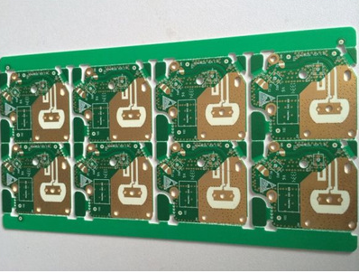
The key production steps of ALV HDI PCB miniaturization are multilayer lamination, laser drilling, imaging, etching and electroplating processes, and how to optimize the process to meet high-volume, robust, reliable and low-cost production.
1. The evolution of micro-hole laser technology
In the mid-1990s, the component pin pitch decreased, and the technical difficulty lies in connecting high-I/O-count components with multi-layer PTH PCBs. In order to meet this challenge, the PCB industry has not only reduced the through holes of mechanical drills to less than 150 mm, but also developed micro-hole technologies, such as photoimageable dielectric layers, plasma etching holes, and laser drilling methods. However, the technology of forming holes by photoimaging requires special photosensitive materials, and plasma has no effect on FR-4. Because of its flexibility, laser drilling has now become the dominant production method.
Initially, the available lasers were TEA CO2 and UV Nd: YAG. There were several shortcomings that limited their practicality and accuracy.
The TEA CO2 laser has a wavelength of 10600 nanometers, it cannot drill copper, its speed is slow, and the pulse is easy to miss. Therefore, there are certain difficulties in application. When using this kind of laser drilling machine, it is necessary to make a window (Conformal Mask) that is as large as or slightly larger than the final laser aperture on the copper surface. In addition, after this long-wavelength laser ablation, a carbonized layer will be formed in the PCB, and this carbonized layer must be removed through relatively strong dross removal parameters.
Later, some companies began to combine CO2 lasers with UV lasers, but this solution is only suitable for PCB prototypes and small batch production. For batch boards, this combined method is not economical and affordable.
In the mid-2000s, industry-leading PCB manufacturers began to develop direct drilling through copper foil. Thin the copper to 5 mm ~ 12 mm thick, and roughen and darken the copper surface before drilling. The technical advantage of this laser direct hole formation is that the step of etching the copper window is reduced, and the cost is significantly reduced. This is today the main method for the production of blind microvias for any layer interconnection. However, the disadvantage of this method is that the processing window is relatively narrow and cannot be reworked. From a quality point of view, it is a huge challenge for the stable mass production of blind microvias smaller than 100 μm. Because defects such as overhanging copper in the orifice, protruding glass fiber and resin residue will cause quality problems in the subsequent desmear and electroplating process, these micro blind holes less than 100 μm must be optimized to remove the overhang copper in the orifice and eliminate them. Defects such as glass fiber protrusion and resin residue.
2. Electroplating and imaging process
The choice of PCB electroplating process is determined by the line width/spacing, the thickness of the insulating layer, and the final copper thickness. In the 0.3 mm pitch BGA design, the diameter of the pad is 150 μm, the blind hole is 75 μm, and two 30 mm/30 mm thin lines are run between the two pads with a pitch of 0.3 mm. It is challenging to make this kind of fine circuit through the existing subtractive method.
Three, ALV HDI technology summary
This article mainly introduces the key process of any layer interconnection PCB board in the production process and its impact on cost. When choosing a process, it should be considered that this technology must meet the current and future needs of electronic packaging products. The challenges faced by HDI PCB are: the increase in PCB functions and the reduction in size, as well as the ultra-thin structure that frequently appears in recent terminal products. In order to prepare materials and production methods in a timely manner, it is necessary to effectively manage the supply chain, shorten the prototype production cycle, and bring their products to the market faster.