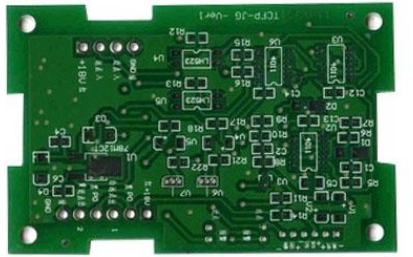
In PCB design and layout, the performance index of a stepper motor drive board is always not up to the performance mentioned in the document. Although it can be used, the high current is lost, the high-speed is not up, and the waveform is poor. After in-depth analysis, it is found that it violates Some of the basic principles of PCB wiring are very good after modification. This makes me feel the importance of PCB wiring again, especially when we often make high-power power supplies and sensors that require extremely strict PCB wiring.
PCB wiring is to lay the roads for power signals to connect various devices. This is like building roads and connecting cities to cars. It's exactly the same thing.
In the PCB layout and design, the wiring switching power supply contains high-frequency signals. Any printed line on the PCB can function as an antenna. The length and width of the printed line will affect its impedance and inductance, thereby affecting the frequency response . Even printed lines that pass DC signals can couple to radio frequency signals from adjacent printed lines and cause circuit problems (even radiating interference signals again). Therefore, all printed lines that pass AC current should be designed to be as short and wide as possible, which means that all components connected to the printed lines and other power lines must be placed very close. The length of the printed line is proportional to its inductance and impedance, and the width is inversely proportional to the inductance and impedance of the printed line. The length reflects the wavelength of the printed line's response. The longer the length, the lower the frequency at which the printed line can send and receive electromagnetic waves, and it can radiate more radio frequency energy. According to the size of the printed circuit board current, try to increase the width of the power line to reduce the loop resistance. At the same time, make the direction of the power line and the ground line consistent with the direction of the current, which helps to enhance the anti-noise ability. Grounding is the bottom branch of the four current loops of the switching power supply. It plays a very important role as a common reference point for the circuit. It is an important method to control interference. Therefore, the placement of the grounding wire should be carefully considered in the layout. Mixing various grounds will cause the power supply to work unstable. Pay attention to the following points in the ground wire design:
1. Correctly choose single-point grounding. Generally, the common end of the filter capacitor should be the only connection point for other grounding points to couple to the high-current AC ground. Should be connected to the grounding point of this level, mainly considering that the current of each part of the circuit returning to the ground is changed, and the impedance of the actual flow of the line will cause the change of the ground potential of each part of the circuit and introduce interference. In this switching power supply, its wiring and the inductance between the devices have a small effect, and the circulating current formed by the grounding circuit has a greater impact on the interference. Connected to the ground pin, the ground wires of several devices that output the current loop of the rectifier are also connected to the ground pins of the corresponding filter capacitors, so that the power supply works more stable and is not easy to self-excite. When a single point is not available, use a common ground Connect two diodes or a small resistor at the place, and it is enough to connect it to a relatively concentrated piece of copper foil.

2. Make the ground wire as thick as possible. If the ground wire is very thin, the ground potential will change with the change of the current, which will cause the timing signal level of the electronic equipment to be unstable and the anti-noise performance to deteriorate, so ensure that each large current ground terminal Use printed lines as short and as wide as possible, and widen the width of the power and ground lines as much as possible. It is best that the ground line is wider than the power line. Their relationship is: ground line>power line>signal line, if possible, ground line The width should be greater than 3mm, and a large area copper layer can also be used as a ground wire. Connect the unused places on the printed circuit board as a ground wire. When performing global wiring, the following principles must also be followed:
(1) PCB wiring direction: From the perspective of the soldering surface, the arrangement of the components should be as consistent as possible with the schematic diagram. The wiring direction is best to be consistent with the wiring direction of the circuit diagram, because it is usually necessary to perform various operations on the soldering surface during the production process. The detection of parameters, so doing so is convenient for inspection, debugging and inspection in production (note: refers to the condition that meets the circuit performance and the requirements of the whole machine installation and panel layout).