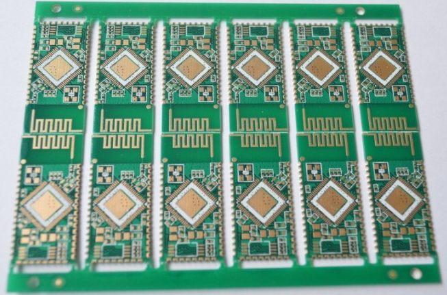
1. The forward design of integrated circuits in PCB design
The design of the integrated circuit is carried out under the condition that the user has clarified the circuit principle, function, various parameter indexes and economic indexes.
The specific process is as follows:
Reverse design of integrated circuits
The concept of reverse design is to completely imitate the existing integrated circuit chip, or to make a partial modification design on the basis of the original chip, or to reduce the area of the original chip and reduce the cost.
specific process:
Design and optimization of household system scheme

We currently provide full system solutions, ranging from high-end GPS, MP3, and tax control machines, to mid-range consumer electronics such as digital radios, home appliance control panels, CNC machine tools and other industrial control products, to low-end toy electronics product. At the same time, we can also perform system integration for users' existing system solutions to further reduce costs and improve the market competitiveness of products.
2. Anatomical analysis of integrated circuits, photomicrographs
It can conduct anatomical analysis and microphotographs of various packaged integrated circuits, and the maximum magnification can reach 4000 times. The specific process is as follows:
3. Memory code point extraction
With the increasing integration of integrated circuits at present, the scale of chips is getting larger and larger. Most of the chips integrate storage devices such as ROM, and use ROM to store user data or programs. The code point extraction of ROM is very important in system design or chip reverse design. ROM code points generally have two forms, one is a plain code, and the other is a mask-type code point. For plain code, we can use our own developed software for direct extraction. For mask-type code points, code point dyeing must be performed first, and then code point extraction. (Successfully extracted more than 32M MASK ROM).
4. Imitation design of surface acoustic wave device (SAW) and high-power tube
Use graphic tools to design surface acoustic wave devices (SAW) and high-power tubes. For surface acoustic wave devices, devices below 2GHZ can be copied, and the geometric error can be controlled within two thousandths. At the same time, it can also produce and package surface acoustic wave devices below 800MHZ. The layout of the high-power tube is generally special, and there are many irregular graphics inside, which can be realized by combining graphics tools with special processing programs.
5. Pads on SMT-PCB
1) For SMT components on the wave soldering surface, the pads of larger components (such as transistors, sockets, etc.) should be appropriately enlarged. For example, the pads of SOT23 can be lengthened by 0.8-1mm to avoid the "shadows" caused by the components. Effect".
2) The size of the PCB pad should be determined according to the size of the component. The width of the pad is equal to or slightly larger than the width of the electrode of the component, and the welding effect is the best.
3). Between two interconnected components, avoid using a single large pad, because the solder on the large pad will connect the two components to the middle. The correct way is to connect the pads of the two components. Separate, connect with a thinner wire between the two pads. If the wire is required to pass a larger current, several wires can be connected in parallel, and the wires are covered with green oil.
4). There must be no through holes on or near the pads of SMT components, otherwise, during the REFLOW process, the solder on the pads will flow along the through holes after melting, which will result in virtual soldering, less tin, and possibly Flow to the other side of the PCB board causes a short circuit.