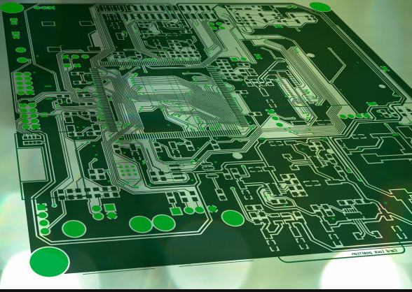
The following introduces the process of Protel DXP drawing PCB board. The whole production process is divided into 16 steps. When we are designing the PCB board, some of these 16 steps are not necessary, but these steps are common in the production of engineering PCB boards, so we will introduce them in detail below.
1 Get the correct schematic and network table
Drawing the schematic diagram is the prerequisite for drawing the PCB board diagram, and the network table is an intermediary connecting the schematic diagram and the PCB board diagram, so you must first get the correct schematic diagram and network table before drawing the PCB circuit board. In addition, we can manually modify the network table to define pads that are not on the schematic diagram such as fixed pins of some components to the network connected to it, and those without any physical connection can be defined to ground or protective ground.
2 Draw the package library of non-standard devices defined by yourself
Packages drawn independently by ourselves must be completed before PCB design. When making PCB circuit boards, we will import these self-made packages.
3 Planning the circuit board

Whether the circuit board is a single-sided board or a multi-layer board, the specific parameters such as the shape and size of the circuit board and the installation method of the circuit board must be considered here. In addition, the interface form between the circuit board and the outside world should be considered, and the package form of the specific connector should be selected.
4 Draw the prohibited wiring layer
Put an appropriate size pad on the place where the fixing hole needs to be placed. For a 3mm screw, a pad with an outer diameter of 6.5-8mm and an inner diameter of 3.2-3.5 can be used. For standard boards, it can be imported from other boards or PCB Wizard.
5 Set environmental parameters
We can set the environmental parameters according to our own habits. Environmental parameters include grid size, cursor capture size, conversion of metric system to imperial system, working level color, etc.
6 Open all the library files to be used and load the netlist file
It should be noted that all the library files must be opened before importing the netlist file. Otherwise, the component will not find the package when importing the netlist.
7 Set working parameters
Mainly carry out the layer setting of the PCB board.
8 Manual layout of components
It should be considered comprehensively from the aspects of mechanical structure, heat dissipation, electromagnetic interference, and the convenience of future wiring. First arrange the components related to the mechanical size and lock these components, then the large components and the core components of the circuit, and then the peripheral small components. For the same device with multiple packaging forms, you can change the packaging of this device to the second packaging form and use the cancel component group function for this device after placing it, and then transfer the netlist again and place the new transfer For this device, there are more types of packaging, and so on. After placing it, you can use the VIEW3D function to check the actual effect.
If you are not satisfied, you can make appropriate adjustments according to the actual situation, and then lock all devices. If the board space permits, you can put some wiring areas similar to the experiment board on the board. For large boards, more fixing screw holes should be added in the middle, and fixing screw holes should also be added to the side of stress-bearing devices such as heavy components or larger connectors on the board. If necessary, some test pads can be placed in appropriate positions. Increase the size of the via hole of the pad that is too small, and define the network of all the fixed screw hole pads to the ground or the protective ground.
9 Develop detailed wiring rules
Wiring rules include the level of use, the line width of each group, the spacing of the vias, the topology of the wiring, etc. We have to set it according to the actual situation of the designed board. In addition, place the FILE filling layer (such as the wiring layer under the radiator and the lying two-pin crystal oscillator) in the area where the wiring is not desired.
10 Manually pre-wire some important lines
For example, circuits such as crystal oscillators, PLLs, and small-signal analog circuits need to be wired manually, and circuits that must be wired according to the specified route must also be manually wired.
11 Automatic wiring
Before automatic wiring, we need to set the automatic wiring function, select the Lock All Pre-Route function among them. This function will not cover our pre-arranged electronic circuits.
If the automatic wiring cannot be completely connected, it can be completed manually or UNDO once. It should be noted that you must not use the undo all wiring function, it will delete all pre-wiring, free pads, and vias. Then we can adjust the layout or wiring rules and re-route. Perform a DRC after completion, and correct any errors. If errors are found in the schematic diagram during the layout and wiring process, the schematic diagram and network table should be updated in time, and the network table should be manually changed and reinstalled before wiring.
12 Adjustment after wiring is completed
After the distribution, make preliminary manual adjustments to the wiring. The contents of adjustment include: manual thickening of ground wires, power wires, power output wires, etc. that need to be thickened; some wires are wound too much and are too cumbersome to redistribute; eliminate some unnecessary vias.
In addition, we have to switch to single-layer display mode to pull the wires of each wiring layer neatly and beautifully. DRC should be performed frequently during manual adjustment, because sometimes some lines will be disconnected. When it is almost finished, each wiring layer can be printed out separately to facilitate the line change. After adjustment, use the VIEW3D function to check the actual effect, and proceed to the next step when satisfied.
13 Copper coating and teardrop
Add teardrops to all vias and pads, and teardrops must be added to patches and single-sided boards. Copper-clad the ground wire network of each wiring layer to enhance the anti-interference ability of the board.
14 DRC inspection
In order to ensure that the circuit board diagram complies with the design rules and all the networks are properly connected, we must conduct DRC inspection after wiring.
15 Adjust the information on the remaining layers
After all adjustments are completed and the DRC is passed, drag and drop all the characters of the silk screen layer to the appropriate position. Be careful not to put them under the components or on the vias or pads. The characters that are too large can be reduced appropriately. Finally, put the name of the printing plate, design version number, company name, date of first processing of the file, name of the printing plate, file processing number and other information, and use the program provided by a third party to add Chinese annotations.
16 Save and export of printed board files
After the Protel DXP draws the PCB circuit board design, we have to finish the printed board file arrangement and archive, and print out the drawings. You can export the component list, generate a spreadsheet document as a component list, and so on. Finally, we have to explain where there are special requirements on the circuit board, and then submit it to the PCB processing factory for circuit board processing.