In the high-speed PCB design, the interference problem in the PCB design of the digital-analog hybrid circuit has always been a difficult problem. In particular, the analog circuit is generally the source of the signal, and whether the signal can be correctly received and converted is an important factor to be considered in the PCB design. The article discusses the general processing method of the digital-analog hybrid circuit by analyzing the mechanism of the interference of the digital-analog hybrid circuit and combining the design practice, and it is verified by design examples.
I. Introduction
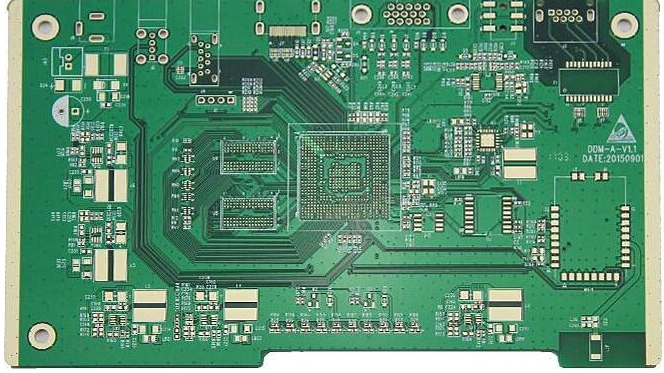
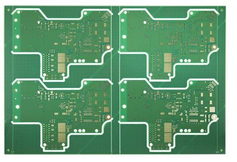
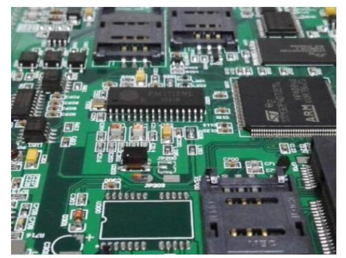
A printed circuit board (PCB) is a support for circuit components and devices in electronic products, and it provides electrical connections between circuit components and devices. Nowadays, many PCBs are no longer single-function circuits, but are composed of a mixture of digital circuits and analog circuits. Data is generally collected and received in an analog circuit, while the bandwidth and gain must be digitized to be controlled by software. Therefore, there are often digital circuits and analog circuits on the same board, and even share the same components. Taking into account the mutual interference between them and the impact on circuit performance, the layout and wiring of the circuit must have certain principles. The special requirements for power transmission lines in mixed-signal PCB design and the requirements for isolating noise coupling between analog and digital circuits have increased the complexity of layout and routing during design. Here, through the analysis of high-density mixed-signal PCB layout and wiring design, to achieve the required PCB design goals.
2. The generation mechanism of digital-analog hybrid circuit interference

Compared with digital signals, analog signals are much more sensitive to noise, because the operation of analog circuits depends on continuously changing current and voltage. Any slight interference can affect its normal operation, while the operation of digital circuits depends on The receiving end detects high level or low level according to a predefined voltage level or threshold, and has a certain anti-interference ability. But in a mixed-signal environment, digital signals are a source of noise relative to analog signals. When the digital circuit is working, the stable effective voltage is only high and low voltage. When the digital logic output changes from a high voltage to a low voltage, the ground pin of the device will discharge and generate a switching current, which is the switching action of the circuit. The faster the speed of the digital circuit, the shorter the switching time is generally required. When a large number of switching circuits change from a logic high level to a logic low level at the same time, due to the insufficient ability of the ground wire to pass current, a large amount of switching current will be caused. The logic ground voltage fluctuates, which we call ground bounce. The ground bounce noise and power disturbance caused by the digital circuit, if coupled to the analog circuit, will affect the performance of the analog circuit. Since quite a lot of interference sources are generated through the power and ground buses, the ground wire causes the largest noise interference, so the design of the ground and power is particularly important when designing the PCB.
Third, the general processing principles of digital-analog hybrid circuit PCB design
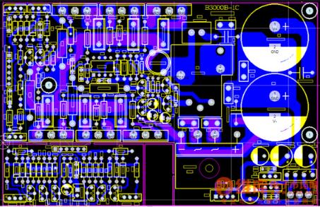
I talked about the mechanism of hybrid circuit interference. How to reduce the mutual interference between digital signal and analog signal? Before designing, we must understand the two basic principles of electromagnetic compatibility (EMC): The first principle is to reduce the area of the current loop as much as possible. If the signal cannot return through the smallest possible loop, a large loop may be formed.状 Antenna. The second principle is that the system uses only one reference plane. On the contrary, if the system has two reference planes, it may form a dipole antenna. Avoid these two situations as much as possible in the design.
(1) The principle of layout and routing. One of the first factors to consider for component layout is to separate the analog circuit part from the digital circuit part. The analog signal is routed in the analog area of all layers of the circuit board, and the digital signal is routed in the digital circuit area. In this case, the digital signal return current will not flow into the analog signal ground. For some high-frequency lines with special requirements, it is best to manually route them, and use differential lines or shielded lines when necessary. Sometimes due to the position of the input/output connector, the wiring of the digital and analog circuits must be mixed together, which may cause the mutual influence of the analog part and the digital part of the circuit. This is necessary to avoid running digital clock lines and high-frequency analog signal lines near the analog power layer, otherwise, the noise of the power signal will be coupled to the sensitive analog signal. To try to achieve a low-impedance power and ground network, the inductance of the digital circuit wire should be minimized, and the capacitive coupling of the analog circuit should be minimized. The frequency of the digital circuit is high, and the sensitivity of the analog circuit is strong. For the signal line, the high-frequency digital signal line should be as far away as possible from the sensitive analog circuit device.
(2) Treatment of power and ground. In the design of complex hybrid circuit boards, the layout and handling of grounding wires are important factors to improve circuit performance. It is suggested to separate the digital ground and analog ground on the mixed-signal circuit board to achieve isolation between the digital ground and the analog ground. However, this method tends to cross the separation gap wiring, which will cause a sharp increase in electromagnetic radiation and signal crosstalk.
Understanding the path and method of current return to ground is the key to optimizing mixed-signal circuit board design. If the ground layer must be divided, and the wiring must be routed through the gap between the divisions, a single-point connection can be made between the divided grounds to form a connection bridge between the two grounds, and then wiring through the connection bridge.