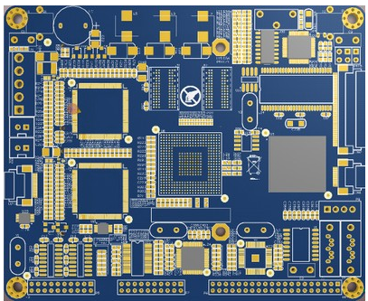
PCBA process: PCBA=Printed Circuit Board Assembly, which means that the empty PCB board passes through SMT and then goes through the entire process of DIP plug-in, referred to as PCBA process.
A printed circuit board
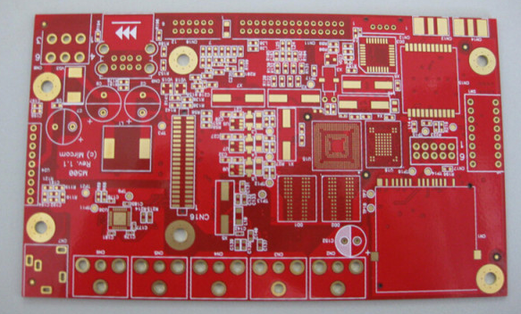
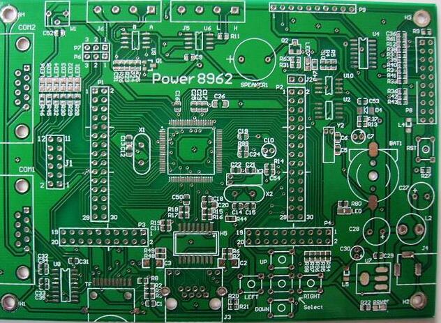
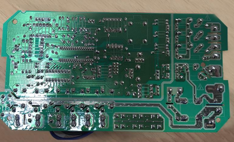
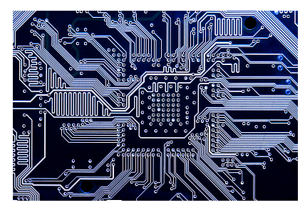
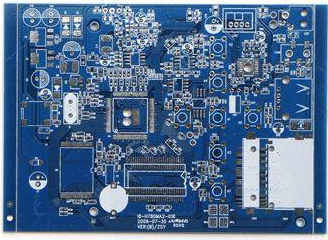
Printed circuit board, also known as printed circuit board, printed circuit board, often use the English abbreviation PCB (Printed circuit board) or write PWB (Printed wire board), is an important electronic component, is the support of electronic components, is the electronic element The provider of the device line connection. The traditional circuit board uses the method of printing etching resist to make the circuit lines and drawings, so it is called a printed circuit board or a printed circuit board. Due to the continuous miniaturization and refinement of electronic products, most of the current circuit boards are attached with etching resists (laminated or coated). After exposure and development, the circuit boards are made by etching.
Technology practical

At the end of the 1990s when numerous build-up printed circuit board solutions were proposed, build-up printed circuit boards have also been put into practical use in large numbers until now.
It is important to develop a robust test strategy for large-scale, high-density printed circuit board assembly (PCBA, printed circuit board assembly) to ensure compliance and functionality with the design. In addition to the establishment and testing of these complex assemblies, the money invested in electronic components alone can be very high-when a unit is finally tested, it can reach $25,000. Due to such high costs, finding and repairing assembly problems is now an even more important step than in the past. Today's more complex assembly is about 18 square inches, 18 layers; there are more than 2,900 components on the top and bottom sides; it contains 6,000 circuit nodes; and there are more than 20,000 solder joints to be tested.
New project development
New development projects require more complex,larger PCBAs and tighter packaging. These requirements challenge our ability to build and test these units. Furthermore, larger circuit boards with smaller components and higher node counts may continue. For example, a design that is currently drawing a circuit board diagram has about 116,000 nodes, more than 5,100 components, and more than 37,800 solder joints that require testing or verification. This unit also has BGA on the top and bottom surfaces, and the BGA is next to each other. Using a traditional needle bed to test a board of this size and complexity, a method of ICT is impossible.
In the manufacturing process, especially in testing, the ever-increasing complexity and density of PCBA is not a new issue. Realizing that increasing the number of test pins in the ICT test fixture is not the way to go, we began to observe alternative circuit verification methods. Seeing the number of non-contact probes per million, we found that at 5000 nodes, many of the errors found (less than 31) may be due to probe contact problems rather than actual manufacturing defects. Therefore, we set out to reduce the number of test pins, rather than increase them. Nevertheless, the quality of our manufacturing process is evaluated to the entire PCBA. We decided that the combination of traditional ICT and X-ray layering is a feasible solution.
Substrate classification
The substrate is generally classified by the insulating part of the substrate. Common raw materials are bakelite, fiberglass board, and various types of plastic boards. PCB manufacturers generally use an insulating part composed of glass fiber, non-woven material, and resin, and then press the epoxy resin and copper foil into a "prepreg" (prepreg) for use.