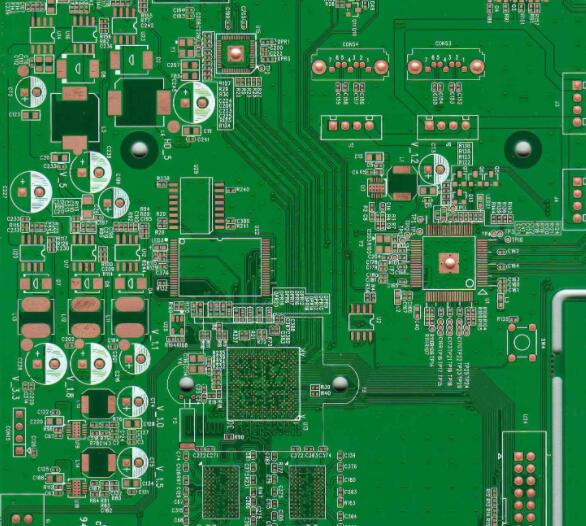
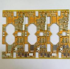
The most basic purpose of PCB surface treatment is to ensure good solderability or electrical properties. Since natural copper tends to exist in the form of oxides in the air, it is unlikely to remain as original copper for a long time, so other treatments are needed for copper.
1. Hot air leveling (spray tin)
Hot air leveling is also known as hot air solder leveling (commonly known as tin spraying). It is a process of coating molten tin (lead) solder on the surface of the PCB and flattening (blowing) it with heated compressed air to form a layer that is resistant to copper oxidation. It can also provide a coating layer with good solderability. During hot air leveling, the solder and copper form a copper-tin intermetallic compound at the joint. When the PCB is leveled with hot air, it must be submerged in the molten solder; the air knife blows the liquid solder before the solder solidifies; the air knife can minimize the meniscus of the solder on the copper surface and prevent the solder from bridging.
Lead spray tin:
The price is cheap, the welding performance is good, the mechanical strength, brightness, etc. Lead is better than lead-free, but it has heavy metals such as lead, which is not environmentally friendly and cannot pass ROHS
Lead-free tin spray:
The price is cheap, but the brightness will be dim compared with lead, and it is environmentally friendly and can pass ROHS

Common disadvantage: not suitable for welding pins with fine gaps and components that are too small, because the surface flatness of the spray tin plate is poor. Solder bead is easy to produce in PCB processing, and it is easy to cause short circuit to fine pitch components. When used in the double-sided SMT process, because the second side has undergone a high-temperature reflow soldering, it is very easy to spray tin and re-melt, resulting in tin beads or similar droplets that are affected by gravity into spherical tin dots, which make the surface even worse. Flattening affects welding problems.
2. Organic Solderability Preservative (OSP)
OSP is a process for surface treatment of printed circuit board (PCB) copper foil that meets the requirements of the RoHS directive. OSP is the abbreviation of Organic Solderability Preservatives, which is translated as Organic Solderability Preservatives in Chinese, also known as Copper Protector, or Preflux in English. Simply put, OSP is to chemically grow a layer of organic film on the clean bare copper surface. This layer of film has anti-oxidation, thermal shock resistance, and moisture resistance to protect the copper surface from rusting (oxidation or sulfidation, etc.) in a normal environment; but in the subsequent welding high temperature, this kind of protective film must be very It is easy to be quickly removed by the flux, so that the exposed clean copper surface can be immediately combined with the molten solder into a strong solder joint in a very short time.
Applicable scenarios: It is estimated that about 25%-30% of PCBs currently use OSP technology, and this proportion has been rising (it is likely that OSP technology has now surpassed tin spraying and ranks first). The OSP process can be used on low-tech PCBs as well as high-tech PCBs, such as PCBs for single-sided TVs and boards for high-density chip packaging. For BGA, OSP has more applications. If PCB does not have functional requirements for surface connection or limitation of storage period, OSP process will be the most ideal surface treatment process.
3, the whole plate is nickel-plated gold
Plating nickel and gold on the PCB surface conductor is plated with a layer of nickel and then with a layer of gold. Nickel plating is mainly to prevent the diffusion between gold and copper. There are two types of electroplated nickel gold now: soft gold plating (pure gold, the gold surface does not look bright) and hard gold plating (the surface is smooth and hard, wear-resistant, contains cobalt and other elements, and the gold surface looks brighter). Soft gold is mainly used for gold wire during chip packaging; hard gold is mainly used for electrical interconnection in non-welded areas.
4. Immersion gold
Immersion gold is a thick, good electrical nickel-gold alloy on the copper surface, which can protect the PCB for a long time; in addition, it also has environmental tolerance that other surface treatment processes do not have. In addition, immersion gold can also prevent the dissolution of copper, which will benefit lead-free assembly.
Advantages: It is not easy to oxidize, can be stored for a long time, and the surface is flat, suitable for welding small gap pins and components with small solder joints. The first choice for PCB boards with buttons (such as mobile phone boards). Reflow soldering can be repeated many times without reducing its solderability. It can be used as a substrate for COB (Chip On Board) wire bonding.
Disadvantages: high cost, poor welding strength, because the electroless nickel plating process is used, it is easy to have the problem of black disk. The nickel layer will oxidize over time, and long-term reliability is a problem.
Applicable scenarios: Immersion gold process is different from OSP process. It is mainly used on boards that have functional connection requirements and a long storage period on the surface, such as mobile phone keypads, edge connection areas of router housings, and chip processors that are elastically connected Electrical contact area. Due to the flatness problem of the tin spraying process and the removal of the flux of the OSP process, immersion gold was widely used in the 1990s; later, due to the appearance of black disks and brittle nickel-phosphorus alloys, the application of immersion gold was reduced., But at present almost every high-tech PCB factory has sinking gold wire.
5. Shen Xi
Since all current solders are tin-based, the tin layer can match any type of solder. The tin sinking process can form a flat copper-tin intermetallic compound. This feature makes the tin sinking have the same good solderability as the hot air leveling without the headache flatness problem of the hot air leveling; the tin plate can not be stored for too long, The assembly must be carried out according to the order of sinking tin.
6. Immersion Silver
Immersion silver process is between organic coating and electroless nickel/immersion gold. The process is relatively simple and fast; even if exposed to heat, humidity and pollution, silver can still maintain good solderability, but will lose its luster . Immersion silver does not have the good physical strength of electroless nickel/immersion gold because there is no nickel under the silver layer.
7. Chemical nickel palladium gold
Compared with immersion gold, chemical nickel palladium gold has an extra layer of palladium between nickel and gold. Palladium can prevent corrosion caused by substitution reaction and make full preparations for immersion gold. Gold is tightly covered on palladium, providing a good contact surface.
8. Plating hard gold
In order to improve the wear resistance of PCB products and increase the number of insertion and removal, hard gold is plated.