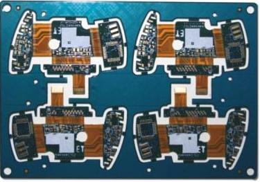
1. The shape and size design standard of the pad in PCB design
The PCB standard package library should be called.
The minimum single side of all pads is not less than 0.25mm, and the maximum diameter of the entire pad is not more than 3 times the component aperture.
Try to ensure that the distance between the edges of the two pads is greater than 0.4mm.
In the case of dense wiring, it is recommended to use oval and oblong connection plates. The diameter or minimum width of the single-sided board pad is 1.6mm; the weak-current circuit pad of the double-sided board only needs to add 0.5mm to the hole diameter. Too large a pad can easily cause unnecessary continuous welding.
The pads with an aperture exceeding 1.2mm or pad diameter exceeding 3.0mm should be designed as diamond or quincunx pads
For plug-in components, in order to avoid the phenomenon of copper foil breaking during welding, and the single-sided connecting plate should be completely covered with copper foil; the minimum requirement for double-sided panels should be filled with teardrops; as shown in the figure:
All machine insert parts need to be designed as drip pads along the bent leg direction to ensure full solder joints at the bent leg.
The pads on the large-area copper skin should be chrysanthemum-shaped pads, not to be soldered. If there is a large area of ground and power lines on the PCB (with an area of more than 500 square millimeters), the window should be partially opened or designed as a grid fill (FILL).

Second, PCB manufacturing process requirements for pads
Test points should be added to the two ends of the chip components that are not connected to the plug-in components. The diameter of the test point is equal to or greater than 1.8mm to facilitate the on-line tester test.
If the IC pin pads with dense pin spacing are not connected to the hand-plug pads, test pads need to be added. For SMD ICs, the test points cannot be placed in the SMD IC silk screen. The diameter of the test point is equal to or greater than 1.8mm to facilitate online tester testing.
If the pad spacing is less than 0.4mm, white oil must be applied to reduce continuous soldering when the wave crest is exceeded.
The two ends and ends of the SMD component should be designed with lead-tin. The lead-tin width is recommended to use 0.5mm wire, and the length is generally 2 or 3mm.
If there are hand-soldering components on the single panel, the tin bath should be removed, the direction is opposite to the soldering direction, and the width of the hole is 0.3MM to 1.0MM; (50-70% of the hole diameter) as shown below:
The spacing and size of the conductive rubber buttons should be consistent with the actual size of the conductive rubber buttons. The PCB board connected to this should be designed as a gold finger, and the corresponding gold plating thickness should be specified.
The size and spacing of the pad should be the same as the size of the chip component (1:1).
For the solder joints with the distance between the pads on the same straight line (the number of pads greater than 4) is less than 0.4mm, on the basis of adding white oil, the long side of the component is as parallel as possible to the direction of the wave crest, then the pad at the end Add an empty pad or enlarge the pad at the end, so as to eat the tail solder and reduce the continuous soldering.