The PCB looks like a multi-layer cake or lasagna-layers of different materials are pressed together by heat and adhesive.
The base material of FR4PCB is generally glass fiber. In most cases, the glass fiber substrate of PCB generally refers to the material "FR4". The solid material "FR4" gives the PCB hardness and thickness. In addition to the FR4 substrate, there are flexible circuit boards produced on flexible high-temperature plastics (polyimide or similar) and so on.
In the production of copper foil layer, heat and adhesive are used to press it onto the substrate. On the double-sided board, the copper foil will be pressed to the front and back sides of the substrate. In some low-cost occasions, copper foil may only be pressed on one side of the substrate. When we refer to "double-sided board" or "two-layer board", we mean that there are two layers of copper foil on our lasagna. Of course, in different PCB designs, the number of copper foil layers may be as few as 1 layer, or more than 16 layers.

one. PCB signal layer
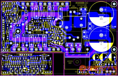
Signal Layers, the signal layer is used to place copper film traces that connect digital or analog signals. The Altium Designer circuit board can have 32 signal layers, where Top is the top layer, Mid1-30 is the middle layer, and Bottom is the bottom layer. Traditionally, the Top layer is also called the component layer, and the Botton layer is also called the soldering layer.
two. Soldermask Layer
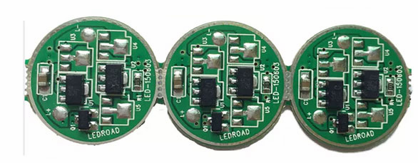
Above the copper layer is the solder mask. This layer makes the PCB look green. The solder mask layer covers the traces on the copper layer to prevent the traces on the PCB from contacting other metals, solder or other conductive objects to cause short circuits. The presence of the solder mask allows everyone to solder in the right place and prevents solder bridging. We can see that the solder mask covers most of the PCB (including the traces), but the silver ring and the tin on the SMD pad are exposed for soldering.
three. Pastemask layer (solder paste protection layer, SMD patch layer)
Its function is similar to that of the solder mask, but the difference is the pad of the corresponding surface-mounted component during machine soldering. Protel99 SE provides two protective layers of solder paste, Top Paste (top layer) and Bottom Paste (bottom layer). Mainly for SMD components on PCB boards. If all Dip (through hole) components are placed on the board, there is no need to export Gerber files on this layer. Before attaching SMD components to the PCB board, solder paste must be applied to each SMD pad. The paste mask file must be used for the steel mesh used for tinning, and the film film can be processed. The most important point of the Gerber output of the Paste Mask layer is to be clear, that is, this layer is mainly for SMD components. At the same time, compare this layer with the Solder Mask described above to find out the different functions of the two, because you can see from the film picture. The two film images are very similar.
Four. Silkscreen Layer
The white characters are the silk screen layer. Letters, numbers and symbols are printed on the silk screen of the PCB, which can facilitate assembly and guide everyone to better understand the design of the board. We often use symbols on the silk screen layer to mark certain pins or LED functions.
five. Mechanical Layer, Keep-Out Layer (outer shape layer and forbidden wiring layer)
The mechanical layer defines the appearance of the entire PCB board. In fact, when we talk about the mechanical layer, we mean the overall appearance of the PCB board. The forbidden wiring layer defines the boundary when we lay out the electrical characteristics of copper. That is to say, after we first define the forbidden wiring layer, in the future wiring process, the wiring with electrical characteristics cannot exceed the forbidden wiring. The boundary of the layer.
six. Drill layer
The drilling layer provides drilling information during the manufacturing process of the PCB circuit board (such as pads and vias need to be drilled). The general file will provide two drilling layers, Drillgride (drilling instruction map) and Drill drawing (drilling drawing).