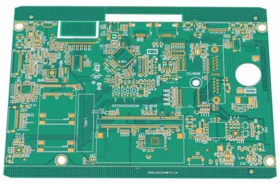
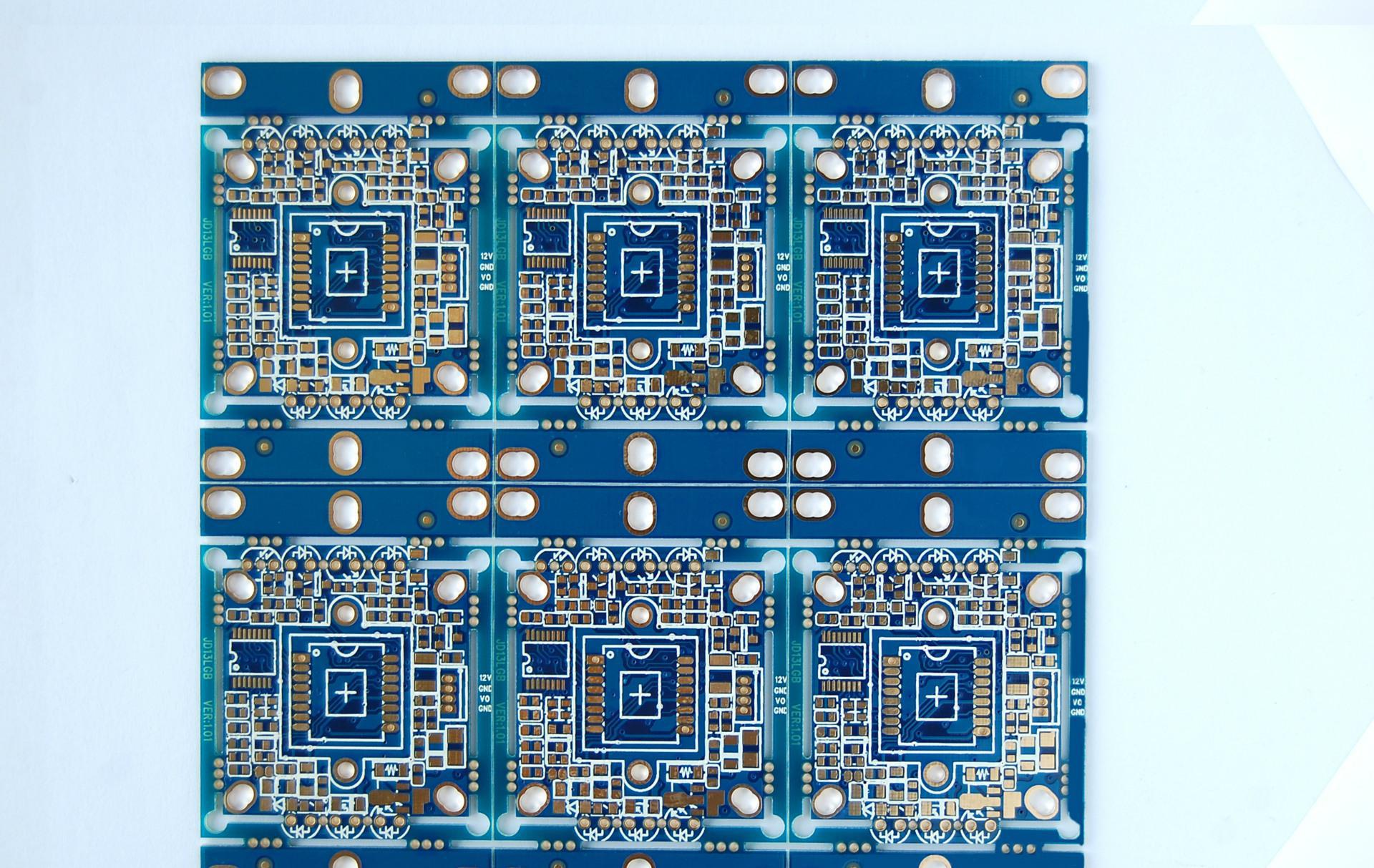
With the development of high-density and high-precision electronic products, corresponding requirements are put forward on circuit boards. The effective way to increase PCB density is to reduce the number of pores and set blind holes. To meet this requirement, HDI boards can be produced. A quick sample of professional 32-layer circuit boards.
1.Halogen-free materials have special functions.
The water absorption performance is 1.1.
The water absorption rate of halogen-free materials is lower than that of ordinary epoxy resins. The main reason is that the isolated electrons of N and P in nitrogen-phosphorus epoxy resins are relatively halogen. The probability of hydrogen bonds forming hydrogen bonds in water is lower than that of halogen materials, so its materials The water absorption rate is lower than that of traditional halogen flame-retardant materials. Reducing the water absorption rate of the material will have a certain impact on the material: professional 32-layer circuit boards.
Improve the reliability of materials.
two. Improve the stability of materials in the PCB process.
Improve the cafe performance of the material.
1.2. The constant of dielectric.

The factors that affect the material's dielectric constant are mainly determined by the following factors: glass fiber dielectric constant, epoxy resin and fillers. The limit of the entire epoxy resin will be reduced to a certain extent, because it is replaced by P or N. Therefore, the electrical insulation of halogen-free epoxy resin will be better than that of halogen epoxy resin. A quick sample of a 32-layer circuit board.
The insulation performance of the material is 1.3.
The halogen-free epoxy resin improves the polarity of the traditional epoxy resin to a certain extent, and improves the insulation resistance and impact resistance of the medium.
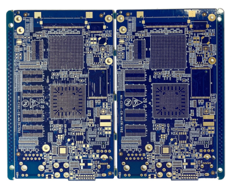
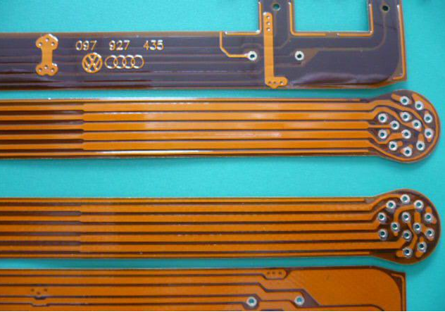
Process flow and technology of buried/blind via multilayer boards.
Generally, the sequential lamination method is used.. That is it.
Opening-forming a core board (equivalent to a traditional double-sided or multi-layer board)-lamination-the following process is the same as that of a traditional multi-layer board.
Note 1: The formation of the core board refers to the double-sided or multi-layer board caused by the traditional method, and the buried/blind-via multi-layer board is formed according to the structural requirements. If the thickness of the chip hole is relatively large, it should be blocked to ensure its reliability. 32-layer circuit board:
When the temperature rises to a certain range, the substrate will change from glass to rubber. At this time, the temperature is called the glass temperature (TG) of the plate. In other words, TG is the base material maintains rigidity * high temperature (C). In other words, ordinary PCB substrate materials not only soften, deform, and melt at high temperatures. At the same time, it also shows a sharp decline in mechanical and electrical characteristics (I think you don’t want to look at the classification of PCB boards, look at your products. Professional 32-layer circuit boards..
Why is the copper foil so thin? There are two main reasons: First, the uniform copper foil has a very uniform temperature coefficient of resistance, which makes the signal transmission loss smaller, which is different from the capacitance requirements. Capacitors require higher dielectric power in order to have a higher capacity in a limited volume. Why are capacitors smaller than aluminum capacitors? After all, the dielectric constant is higher. Second, the temperature of thin copper foil rises under high current conditions, which is conducive to heat dissipation and component life. In digital integrated circuits, the same is true for copper wire widths less than 0.3cm. The well-made PCB finished board is very uniform, and the gloss is soft (because the surface is brushed with solder resist) can be seen with the naked eye. A quick sample of a 32-layer circuit board.
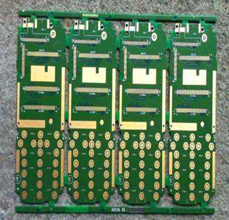
Dingji Electronics is a company specializing in the processing and production of printed circuit boards, with the advantages of single-sided printed circuit boards, double-sided printed circuit boards, and multilayer printed circuit boards. It can provide high-quality, high-precision eight-layer circuit board production.
The holes and blind holes above eight layers are opened from the top layer to the bottom layer, and the blind holes are only invisible on the top layer or the bottom layer. In other words, blind holes are drilled from the surface instead of penetrating all layers. Another type of hole called buried hole means that the bottom of the inner layer through hole is invisible. The advantage of buried vias and blind vias is that they can increase wiring space.