The wiring of the PCI card is more exquisite, which is determined by the characteristics of the PCI signal. In the conventional high-frequency digital PCB circuit board design, we always strive to avoid signal reflection, overshoot, ringing, and non-monotonic phenomena caused by impedance mismatch. However, PCI signals use the principle of signal reflection to transmit physical Signal, in order to make reasonable use of signal reflection while trying to avoid side effects such as large overshoot, ringing and non-monotonicity, PCI-SIG has made some provisions on PCB physical realization in the PCI specification.

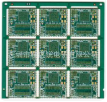
PCI-SIG recommends the use of a four-layer PCB board for PCI cards. The signal distribution of PCI connectors specified by PCI-SIG is also optimized for the convenience of four-layer board wiring. PCI-SIG has also made a recommended schematic diagram for the pin distribution of PCI controllers. In fact, PCI controller manufacturers such as AMCC, PLX, and OXFORD have also implemented this recommendation. Under this recommended pin distribution, two layers are used. The PCB board is actually very convenient for wiring, but if the PCI card system hardware is very complex and requires multiple power split levels, it is better to have a multi-layer PCB.
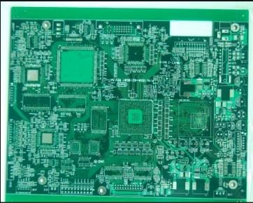
Any PCI signal on the PCI card can only be connected to one load (including also cannot be connected to a pull-up resistor). Except for CLK, RST, INTA#~INTD#, JTAG these pins, all pins from the contact point of the golden finger and the card socket to the load end shall not be larger than 1.5 inches; the length of the CLK signal is 2.5 +-0.1 inch, this length It's a bit long, so in many cases it needs to be routed around to meet the length requirement. This is why you often see the serpentine trace of CLK on the PCI card; there are no special regulations for the remaining pins. When using a multi-layer PCB, the signal traces should not cross different power levels (at least, the layer with the split power level should be on the other side of the PCB), which is why we often see all the gold fingers on the A side of the PCI card come up The reason why the signal often goes to the B side (component side) through a hole.
The characteristic impedance of each PCI signal is 60-100 ohms, and the load capacitance must not exceed 10pf. The IO Pad of the IC should be able to withstand -3.5V undershoot and +7.1V signal overshoot. For PCI controller manufacturers such as AMCC, PLX, and OXFORD, the controller IC meets these regulations, and users do not need to consider it. However, if you use CPLD/FPGA to implement the PCI controller, you must consider whether the model used meets these regulations. CPLD/FPGA manufacturers such as Altera and Xilinx will clearly state in their data manuals whether the CPLD/FPGA is compatible with PCI signal specifications.
Well, the wiring of the ordinary 32-bit 33MHz PCI card is relatively simple, mainly to meet the length requirements. In fact, if you do not strictly follow the wiring requirements, there will generally be no problems, but depending on the motherboard chipset, once the signal compatibility problem occurs, the hardware debugging of the PCI card will be the most painful experience in the PCB circuit design. .