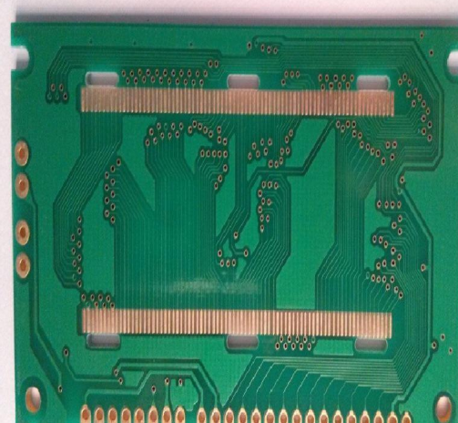
One of the tools used in signal integrity analysis is modeling. We will use this analysis tool here to first build a model for the PCB transmission line, and then analyze its various behavioral characteristics.
The zero-order model of the PCB transmission line is the simplest and most understandable model. It is composed of a row of miniature capacitors in parallel, and the value is equal to the capacitance per unit length of the PCB transmission line.
The following describes how to use the zero-order model of the PCB transmission line to analyze the voltage-current (V-I) characteristics and transient impedance of the PCB transmission line.
Suppose the unit length is △X, and the size of each miniature capacitor is the product of the capacitance per unit length of the PCB transmission line and the unit length:
C=Co*△X (3-5)

The current I is determined by the power Q injected into each capacitor. The power Q injected into the capacitor is equal to the capacitor C multiplied by the voltage V across it. The time interval for the power to be injected into each microcapacitor is △t, which is equal to the unit length △X divided by the signal propagation speed υ. The current I can be expressed by the following formula:
It can be seen that the current on the wire is only related to the capacitance per unit length, the propagation speed of the signal and the voltage. The voltage-current (V-I) characteristics of the PCB transmission line: the instantaneous current at any = on the PCB transmission line is proportional to the voltage.
After obtaining the current of the PCB transmission line, the transient impedance of the signal can be derived, according to Ohm’s law
In the actual calculation, the speed of light in the material is taken into the above formula to obtain
It can be seen from the above formula that the transient impedance of the PCB transmission line is only determined by the cross-sectional area of the PCB transmission line and the material characteristics, that is, the dielectric constant, and the unit is Ω.
Example: If the dielectric constant is 9, the capacitance per unit length is 4.98 pF/in, then the transient impedance of the PCB transmission line is
If the above two characteristic parameters of the PCB transmission line remain unchanged, no matter how the length of the PCB transmission line changes, the transient impedance is always a fixed value.
The zero-order model describes the PCB transmission line as a series of miniature capacitors separated by a certain distance. This is only the physical model of the PCB transmission line. In order to obtain its equivalent electrical model, the first-order model of the PCB transmission line is introduced next.
The first-order model is based on the zero-order model. Each small section of the two wires of the PCB transmission line is replaced by an inductor, and every two parallel microcapacitors are connected by inductors to form a micro-segment.
The basic idea of the classic PCB transmission line analysis theory is: the circuit parameters of a uniform PCB transmission line are evenly distributed on the PCB transmission line, so the voltage on the PCB transmission line is not only a function of time t, but also a function of space coordinate x, that is, at distance At the beginning x, a micro-segment with a curved length is used to study. When dx is small enough, the distribution of circuit parameters on this segment can be ignored, and the lumped parameter circuit can be used as equivalent replacement. In this way, the entire uniform PCB transmission line can be regarded as a series of such The micro segments are cascaded. As it involves differential equations, from a practical point of view, it will not be introduced here. Readers can refer to the literature of relevant PCB transmission line theory.
In order to simplify the analysis of the first-order model, it is assumed that the capacitance and inductance are infinitely small; the number of sections of the LC circuit tends to be infinite; the unit length capacitance Co and the unit length inductance Lo are constants; the total length of the PCB transmission line is ι; then the total capacitance and inductance Respectively
C=Co*ι (3-11)
L=Lo*ι (3-12)
Derive the capacitance per unit length and the inductance per unit length from the characteristic impedance Zo and the velocity v as follows
The delay and characteristic impedance of the PCB transmission line derive the total capacitance and total inductance as follows
It can be known from the network theory that when a signal is transmitted along the network, it is subjected to a constant transient impedance at each node, and there will be a certain time delay for the signal from the input network to the output network. Equations (3-13) and (3-14) can support this conclusion.
In order to avoid cumbersome theory and differential equation derivation, some practical calculation formulas for the first-order model are given for readers to refer to in the future.
The above-mentioned relations are applicable to all PCB transmission lines and have nothing to do with their geometry. If you know two of them, you can find all the other parameters, which is very convenient and practical.