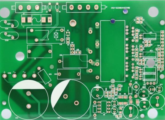
In view of the effects introduced by the high-speed PCB transmission line problem, we will talk about the methods to control these effects from the following aspects.
1 Strictly control the length of key network cables
If there is a high-speed transition edge in the design, the problem of the transmission line effect on the PCB must be considered. Fast integrated circuit chips with very high clock frequencies that are commonly used nowadays have such problems. There are some basic principles to solve this problem: if CMOS or TTL circuits are used for design, the operating frequency is less than 10MHz, and the wiring length should not be greater than 7 inches. The wiring length should not be greater than 1.5 inches at 50MHz. If the operating frequency reaches or exceeds 75MHz, the wiring length should be 1 inch. The maximum wiring length for GaAs chips should be 0.3 inches. If this standard is exceeded, there will be transmission line problems.
2 Reasonably plan the topology of the wiring
Another way to solve the effect of high-speed PCB transmission lines is to select the correct wiring path and terminal topology. The topological structure of the wiring refers to the wiring sequence and wiring structure of a network cable. When using high-speed logic devices, unless the length of the trace branch is kept short, signals with rapidly changing edges will be distorted by the branch traces on the signal trunk trace. Under normal circumstances, PCB routing uses two basic topologies, namely Daisy Chain routing and Star distribution.

For daisy chain wiring, the wiring starts from the driving end and reaches each receiving end in turn. If a series resistance is used to change the signal characteristics, the position of the series resistance should be close to the drive end. In terms of controlling the high-order harmonic interference of the wiring, the daisy chain wiring has the best effect. However, this wiring method has the lowest distribution rate, and it is not easy to distribute 100%. In the actual design, we make the branch length in the daisy chain wiring as short as possible. The safe length value should be: Stub Delay <= Trt *0.1.
For example, the length of the branch end in a high-speed TTL circuit should be less than 1.5 inches. This topology occupies less wiring space and can be terminated with a single resistor. However, this wiring structure makes the reception of signals at different signal receiving ends asynchronous.
The star topology structure can effectively avoid the asynchronous problem of the clock signal, but it is very difficult to manually complete the wiring on the high-density PCB board. Using an automatic router is the best way to complete star wiring. Terminating resistors are required on each branch. The resistance of the terminal resistor should match the characteristic impedance of the connection. This can be calculated manually or by CAD tools to calculate the characteristic impedance value and the terminal matching resistance value.
In the above two examples, simple terminal resistors are used. In practice, more complex matching terminals can be selected. The first option is RC matching terminal. The RC matching terminal can reduce power consumption, but it can only be used when the signal is relatively stable. This method is most suitable for matching the clock line signal. The disadvantage is that the capacitance in the RC matching terminal may affect the shape and propagation speed of the signal.
The series resistance matching terminal will not produce additional power consumption, but will slow down the signal transmission. This method is used for bus drive circuits where the time delay has little effect. The advantage of the series resistance matching terminal is that it can reduce the number of on-board devices and the density of wiring.
The last method is to separate the matching terminal. In this way, the matching component needs to be placed near the receiving end. The advantage is that it will not pull down the signal, and noise can be avoided very well. Typically used for TTL input signals (ACT, HCT, FAST).
In addition, the package type and installation type of the terminal matching resistor must also be considered. Generally, SMD surface mount resistors have lower inductance than through-hole components, so SMD packaged components become the first choice. If you choose ordinary in-line resistors, there are also two options for installation: vertical and horizontal.
In the vertical installation mode, one mounting pin of the resistor is very short, which can reduce the thermal resistance between the resistor and the circuit board, so that the heat of the resistor can be more easily dissipated into the air. But a longer vertical installation will increase the inductance of the resistor. Horizontal installation has lower inductance due to lower installation. However, the overheated resistance will drift. In the worst case, the resistance will become an open circuit, causing the PCB trace termination matching failure and becoming a potential failure factor.
3 Methods to suppress electromagnetic interference
A good solution to the signal integrity problem will improve the electromagnetic compatibility (EMC) of the PCB board. One of the very important is to ensure that the PCB board has a good grounding. It is very effective to use a signal layer with a ground layer for complex designs. In addition, minimizing the signal density of the outermost layer of the circuit board is also a good way to reduce electromagnetic radiation. This method can be realized by using the "surface area layer" technology "Build-up" design and manufacturing PCB. The surface area layer is realized by adding a combination of a thin insulating layer and micro-holes used to penetrate these layers on a common process PCB. The resistance and capacitance can be buried under the surface layer, and the trace density per unit area will be nearly doubled. Reduce the size of the PCB. The reduction of PCB area has a huge impact on the topological structure of the trace, which means that the current loop is reduced, the length of the branch trace is reduced, and the electromagnetic radiation is approximately proportional to the area of the current loop; at the same time, the small size feature means high-density lead Foot-packaged devices can be used, which in turn reduces the length of the wire, thereby reducing the current loop and improving the electromagnetic compatibility characteristics.
4 Other available technologies
In order to reduce the instantaneous overshoot of the voltage on the power supply of the integrated circuit chip, a decoupling capacitor should be added to the integrated circuit chip. This can effectively remove the effects of burrs on the power supply and reduce the radiation of the power loop on the printed board.
When the decoupling capacitor is directly connected to the power tube leg of the integrated circuit instead of the power layer, the effect of smoothing the burr is best. This is why some device sockets have decoupling capacitors, and some devices require the distance between the decoupling capacitor and the device to be small enough.
Any high-speed and high-power devices should be placed together as much as possible to reduce the transient overshoot of the power supply voltage.
If there is no power layer, the long power connection will form a loop between the signal and the loop, becoming a radiation source and a sensitive circuit.
The situation where the PCB traces form a loop that does not pass through the same network cable or other traces is called an open loop. If the loop passes through other wires of the same network cable, it constitutes a closed loop. In both cases, antenna effects (wire antennas and loop antennas) are formed. The antenna generates EMI radiation externally and is also a sensitive circuit itself. The closed loop is a problem that must be considered because the radiation it generates is approximately proportional to the area of the closed loop.