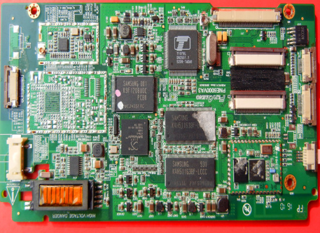
According to the transmission line model, to sum up, the transmission line will bring the following effects to the entire high-speed PCB circuit design.
5.1 Reflected signal
If a trace is not properly terminated (terminal matching), then the signal pulse from the driving end is reflected at the receiving end, causing unexpected effects and distorting the signal profile. When the distortion is very significant, it can cause a variety of errors and cause design failure. At the same time, the susceptibility of the distorted signal to noise increases, which can also cause design failure. If the above situation is not considered enough, EMI will increase significantly, which will not only affect the results of its own design, but also cause the failure of the entire system. The main reasons for reflected signals are: too long traces; transmission lines that are not terminated by matching, excessive capacitance or inductance, and impedance mismatch.
5.2 Delay and timing errors
Signal delay and timing errors are manifested as: the signal does not jump for a period of time when the signal changes between the high and low thresholds of the logic level. Excessive signal delay may cause timing errors and confusion of device functions.

Problems usually arise when there are multiple receivers. The PCB circuit designer must determine the worst-case time delay to ensure the correctness of the design. The reason for the signal delay: the driver is overloaded, and the wiring is too long.
5.3 Multiple times of crossing the logic level threshold error
The signal may cross the logic level threshold many times during the transition process, resulting in this type of error. The error of crossing the logic level threshold multiple times is a special form of signal oscillation, that is, the oscillation of the signal occurs near the logic level threshold, and crossing the logic level threshold multiple times will cause the logic function disorder. Causes of reflected signals: long traces, unterminated transmission lines, excessive capacitance or inductance, and impedance mismatch.
5.4 Overshoot and undershoot
Overshoot and undershoot come from two reasons: the trace is too long or the signal changes too fast. Although most component receiving ends are protected by input protection diodes, sometimes these overshoot levels will far exceed the component power supply voltage range and damage components.
5.5 Crosstalk
Crosstalk is manifested as when a signal passes through a signal line, the relevant signal will be induced on the signal line adjacent to it on the PCB board. We call it crosstalk. The closer the signal line is to the ground, the greater the line spacing, and the smaller the crosstalk signal generated. Asynchronous signals and clock signals are more prone to crosstalk. Therefore, the method of crosstalk removal is to remove the crosstalk signal or shield the signal that is seriously interfered.
5.6 Electromagnetic radiation
EMI (Electro-Magnetic Interference) refers to electromagnetic interference. The problems caused include excessive electromagnetic radiation and susceptibility to electromagnetic radiation. EMI is manifested in that when a digital system is powered on, it will radiate electromagnetic waves to the surrounding environment, thereby interfering with the normal operation of electronic equipment in the surrounding environment. The main reason for it is that the operating frequency of the circuit is too high and the layout is unreasonable. There are software tools for EMI simulation, but EMI simulators are very expensive, and it is difficult to set simulation parameters and boundary conditions, which will directly affect the accuracy and practicability of the simulation results. The most common method is to apply various design rules for controlling EMI in every aspect of the design, and realize the rule drive and control in every aspect of PCB design.