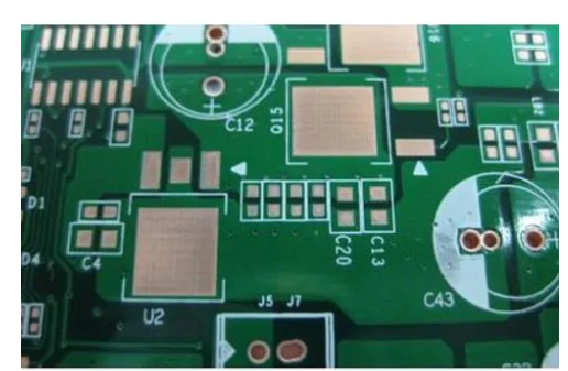
1. Green paint construction
The ball-planting pad on the bottom of the BGA belly is welded using the "green paint set limit" method. Once the green paint is too thick (above 1mil) and the backing surface is too small, there will be a "crater effect" that is difficult for wave soldering to enter. In addition, under the attack of a large amount of flux and high heat in the ball planting operation of the cutting board, the solder will be forced to penetrate into the bottom of the edge of the green paint, which may cause the green paint to float away. This point is quite different from that of solder paste soldering on PCB processing pads. Usually, the SMD copper pad of this kind of carrier board will be slightly larger (sometimes containing nickel and gold), the green paint can climb up to the 4mil peripheral width of the circumference, because the tin can not flow to the outer straight wall of the copper pad, so stress is recommended. Its strength is not as good as the NSMD solder joints formed by all copper pads. In addition, the stress of SMD solder joints is not easy to dissipate, resulting in its "fatigue life" generally being only 70% of NSMD. In fact, the designers and manufacturers of general packaging substrates do not know much about this logic. As a result, the strength of various BGAs on the PCB circuit boards of mobile phones will be increasingly unsafe in the future for lead-free soldering.
(1) Green paint plug hole

Usually the function of the green paint plug hole is to facilitate the removal of the empty space to quickly fix the board when testing the PCB circuit board; secondly, it is for the circuit or solder pad near the through hole on the first side to avoid the second surface wave soldering. Violated by Yong Tin. However, if the plug is not firm and broken, it will still suffer from endless troubles caused by the strong pressure into the tin dross by spraying tin or wave soldering. There were four plug hole methods listed in the original table, but none of them are practical in mass production.
(2) Wave welding again after fusion welding
When the welding of some parts is completed on both sides, some PCB components are often required to be soldered, so that the through holes adjacent to the ball pad will also transfer the heat of the wave soldering to the first side, causing the bottom of the belly to be Reflowed. The soldered ball may be remelted again, and may even form an accidental cold weld or open circuit. At this time, the temporary Heat Shield and Wave Shield two kinds of external heat shields can be used to insulate the upper and lower sides of the BGA area.
(3) Construction of plugging holes
Green paint hole plugging construction methods include: dry film cover hole, printing flooded hole, which means that the hole is inserted into the printing plate surface by the way. come out. Professional plug holes are plugged and cured deliberately using special resin, and then green paint is printed on both sides. No matter what the method is, it can be called a difficult construction method that is not easy to perfect. As a result, the front or back plugs of OSP boards with green paint do not work, and there are many cases of miserable failures downstream. When OSP is made after the front plug, it is easy to leave the liquid medicine in the slit and damage the perforated copper, and the baking of the back plug will be detrimental to the OSP film, which is indeed a dilemma.
Second, the placement of BGA
(1) Printing of solder paste
The opening of the steel plate used is best to adopt a narrow and wide trapezoidal opening to facilitate stepping on the foot and raising the steel plate after printing without disturbing the solder paste. The metal part of the commonly used solder paste accounts for about 90%, and the size of the solder particles should not exceed 24% of the opening to avoid blurring the edges of the paste. The most commonly used BGA assembly printing paste has a particle size of 53μm, while CSP has a commonly used particle size of 38μm.
For large-scale BGA with a pitch of 1.0-1.5mm, the thickness of the printed steel plate should be 0.15-0.18mm, and for a BGA with a fine pitch of less than 0.8mm, the thickness of the steel plate should be reduced to 0.1-0.15mm. The "aspect ratio" of the opening must be kept at about 1.5 to facilitate the application of the paste. The corners of the openings of the square pads of the close-spacers must be arced to reduce the sticking of the tin particles. For small-pitch round pads, once the steel plate width to depth ratio must be less than 66%, the printed paste must be 2-3 mils larger than the pad surface, so that the temporary adhesion before welding is better.
(Two), hot air fusion welding
After 90 years, forced convection hot air has become the mainstream of Reflow. The more heating sections in its production line, it is not only easy to adjust the "temperature-time curve", but also the production speed will be accelerated. Current lead-free solderers must have an average of more than 10 segments to facilitate heating (up to 14 segments). When the high temperature in the profile has exceeded the Tg of the plate and gets along for too long, it will not only make the PCB circuit board soft, but also the Z expansion will cause the board to burst, resulting in disasters such as inner circuit or PTH fracture. The flux in the solder paste must be above 130°C to show its activity, and its activation time can be maintained for 90-120 seconds. The average heat resistance limit of various components is 220°C and cannot exceed 60 seconds.