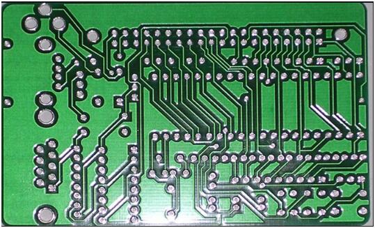
In the PCB circuit board design, if the designer wants to achieve the desired effect, he must master good design skills on the basis of familiarity with professional knowledge. Today I will tell you about five small details that you need to pay attention to in PCB circuit board design.
1. It is the oil problem of the via hole cover. For the via cap oil required by the user, the designer should pay attention to checking the drawings during the design, and must not treat the cap oil as a window opening, otherwise the final product must also be windowed.
2. It is the problem of golden hands opening the window. If you want to open the window treatment, you should make a clear mark in the drawing design to ensure that it is not designed to be covered with oil. Generally speaking, golden fingers are used to open windows, and users need to make clear marks if they have special requirements.

3. It is the line layout problem. In order to prevent mutual interference, the directions of the lines should be parallel and not cross each other. The designer should ensure that the lines have a reasonable direction during the design process to further improve the rationality and feasibility of the design.
4. It is a character problem. Characters printed smaller than the minimum size will be unclear. Generally speaking, the smallest character size is 0.8*1.5MM. In addition, characters cannot be placed on the pad, and all characters on the pad should be removed.
5. It is the problem of power filter layout. The layout of the power supply filter should be as close as possible to the switching device or other components that need to be filtered. If it is too far away, it will lose its function. In addition, when the power supply filter is properly arranged, the problem of the grounding point becomes less obvious.
6. The distribution of PCB wiring layers and plane layers requires symmetrical up and down from the center line of the PCB stack (including the number of layers, the distance from the center line, the copper thickness of the wiring layer and other parameters)
Note: The PCB stacking method requires a symmetrical design. The symmetrical design refers to the thickness of the insulation layer, the type of prepreg, the thickness of the copper foil, and the pattern distribution type (large copper foil layer, circuit layer) as symmetrical to the center line of the PCB as possible.
7. The design of line width and dielectric thickness needs to leave sufficient margin to avoid design problems such as SI caused by insufficient margin
The stack of PCB is composed of power layer, ground layer and signal layer. As the name suggests, the signal layer is the wiring layer of the signal line. The power layer and the ground layer are sometimes collectively referred to as the plane layer.
In a small number of PCB designs, wiring on the power ground plane layer or power and ground network on the wiring layer is used. For this mixed type of layer design, it is collectively called the signal layer.