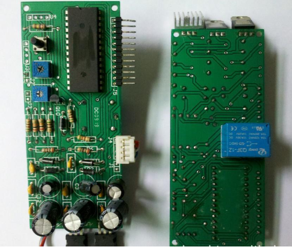
Before soldering BGA, both PCB and BGA should be baked in a constant temperature oven at 80 degree Celsius~90 degree Celsius for 10~20 hours. The purpose is to remove moisture and adjust the baking temperature and time appropriately depending on the degree of moisture. PCB and BGA without unpacking can be soldered directly. In particular, when performing all the following operations, wear an electrostatic ring or anti-static gloves to avoid possible damage to the chip caused by static electricity. Before soldering the BGA, it is necessary to accurately align the BGA on the pads on the PCB. Two methods are used here: optical alignment and manual alignment. At present, manual alignment is mainly used, which is to align the circumference of the BGA with the silk screen around on the PCB pad. Here is a trick: In the process of aligning the BGA and the silk screen line, even if they are not completely aligned, even if the solder ball and the pad deviate by about 30%, soldering can still be performed. Because the solder ball will automatically align with the pad due to the tension between it and the pad during the melting process. After completing the alignment operation, place the PCB on the bracket of the BGA rework station and fix it so that it is level with the BGA rework station. Select the appropriate hot air nozzle (that is, the nozzle size is slightly larger than the BGA size), and then select the corresponding temperature profile, start welding, after the temperature profile is completed, cool down, then the BGA welding is completed.
The following is an introduction to 4 special plating methods in PCB circuit board welding

■Finger row electroplating
It is often necessary to plate rare metals on board edge connectors, board edge protruding contacts, or gold fingers to provide lower contact resistance and higher wear resistance. This technique is called finger row plating or protruding part plating. Gold is often plated on the protruding contacts of the board edge connector with the inner plating layer of nickel. The gold fingers or the protruding parts of the board edge are manually or automatically plated. At present, the gold plating on the contact plug or gold finger has been plated or leaded., Instead of plated buttons. The process is as follows:
1) Strip the coating to remove the tin or tin-lead coating on the protruding contacts
2) Rinse with washing water
3) Scrubbing with abrasives
4) The activation is diffused in 10% sulfuric acid
5) The thickness of nickel plating on the protruding contacts is 4 -5μm
6) Clean and demineralize water
7) Gold penetration solution treatment
8) Gold plated
9) Cleaning
10) Drying
■PCB Through Hole Plating
There are many ways to build a layer of electroplating layer that meets the requirements on the hole wall of the substrate drilled hole. This is called hole wall activation in industrial applications. The commercial production process of its printed circuit requires multiple intermediate storage tanks. The tank has its own control and maintenance requirements. Through hole plating is a necessary follow-up process of the drilling process. When the drill bit drills through the copper foil and the substrate underneath, the heat generated melts the insulating synthetic resin that constitutes most of the substrate matrix, the molten resin and other drilling debris It accumulates around the hole and is coated on the newly exposed hole wall in the copper foil. In fact, this is harmful to the subsequent electroplating surface. The molten resin will also leave a layer of hot shaft on the hole wall of the substrate, which exhibits poor adhesion to most activators, which requires the development of a class of similar decontamination and etch-back chemical technologies.
A more suitable method for PCB prototyping is to use a specially designed low-viscosity ink to form a high-adhesion, high-conductivity film on the inner wall of each through hole. In this way, there is no need to use multiple chemical treatment processes, only one application step, followed by thermal curing, can form a continuous film on the inner side of all the hole walls, which can be directly electroplated without further treatment. This ink is a resin-based substance that has strong adhesion and can be easily adhered to the walls of most thermally polished holes, thus eliminating the step of etch-back.
■Reel linkage type selective plating
The pins and pins of electronic components, such as connectors, integrated circuits, transistors, and flexible printed circuits, all use selective plating to obtain good contact resistance and corrosion resistance. This electroplating method can be manual or automatic. It is very expensive to selectively plate each pin individually, so batch welding must be used. Usually, the two ends of the metal foil that is rolled to the required thickness are punched, cleaned by chemical or mechanical methods, and then selectively used such as nickel, gold, silver, rhodium, button or tin-nickel alloy, copper-nickel alloy, Nickel-lead alloy, etc. for continuous electroplating. In the electroplating method of selective plating, first coat a layer of resist film on the part of the metal copper foil board that does not need to be electroplated, and electroplating only on the selected part of the copper foil.
■Brush Plating
Another method of selective plating is called "brush plating". It is an electrodeposition technique, and not all parts are immersed in the electrolyte during the electroplating process. In this kind of electroplating technology, only a limited area is electroplated, and there is no effect on the rest. Usually, rare metals are plated on selected parts of the PCB circuit board, such as areas such as board edge connectors. Brush plating is used more when repairing discarded circuit boards in electronic assembly workshops. Wrap a special anode (a chemically inactive anode, such as graphite) in an absorbent material (cotton swab), and use it to bring the electroplating solution to the place where electroplating is needed.