The reason for the interfacial tension of spot welding in PCBA patch processing: the interfacial tension of a certain surface layer lies in the bonding energy between atoms. In most shape memory alloys, each molecule has about 12 neighboring molecules, which can be regarded as the sum of the bonding energy between these atoms. Surface molecules have higher potential energy than body molecules, because the molecules surrounding it are not complete. If the total area of the surface layer expands, a large number of molecules occupy the area on the surface layer, and the kinetic energy consumed will increase. The bonding energy of a molecule is closely related to the latent heat of vaporization. To vaporize a molecule, all molecular bonds adjacent to it must be opened. In order to better move a molecule from the body to the surface layer, a part of the bonds of this molecule must be opened. Therefore, there is a certain kind of correlation between the latent heat of vaporization and the interfacial tension. The compressive strength of interatomic bonds is also reflected in the melting point.

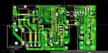
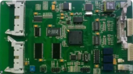
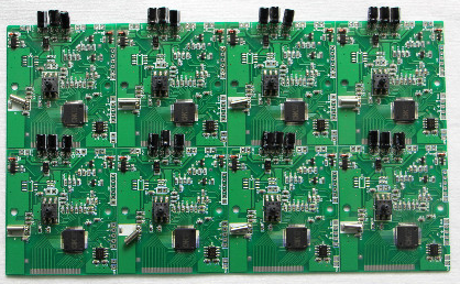
Metal materials always have strong interfacial tension. The hazard of interfacial tension to the surface design of liquid welding materials. The surface contours of liquid welding materials can be calculated and measured according to the working pressure equations of the Laplace equation library. This problem is not discussed in depth here, but only Three pictures are shown. Master the design is determined by the surface activation energy. Contact the PCBA patch spot welding, if the PCB factory understands that the appearance design of the SMT patch processing spot welding follows a certain regularity, it is related to the structure of the spot welding and the interfacial tension of the molten welding material, just like piled gravel, sand The inclination of the pile is constant. The occurrence of spot welding in PCBA patch processing is not a thorough reflection of the welding material drop and the page, but the reflection of the melting welding material and the page that is slowly vaporized by the thermal conductivity of the component package and the cover, and the circuit board processing The spot welding contour is dynamically generated as the solder paste gradually melts. Although the subsequent appearance design is the same as that of the liquid soldering material, it has a full process in the middle.
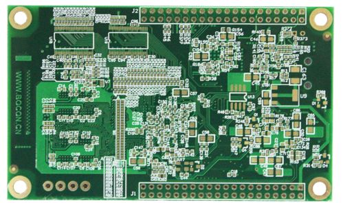
This whole process in the middle is very much related to the qualified rate of electric welding. New machinery and equipment are needed, and the capital investment of new machinery and equipment requires PCBA processing plants to continuously improve the working ability of SMT patch processing technology, and to improve the training and specific guidance of technical personnel. To ensure the standardization of the quality of electric welding, to improve the credibility and reliability of the product. However, from the perspective of PCB circuit board processing, the crack rate cannot be prevented. None of the manufacturers can say that there is no crack in their own patch welding. So what is causing the cracks? Solder paste. The aluminum alloy composition of the solder paste is different, and the size of the particles will cause the bubble to flow back to the welding process during the whole process of the solder paste packaging and printing. crack.
PCB solder layer metal surface treatment method. The surface treatment of the weld layer metal also has a particularly important hazard for causing cracks. Flow back curve setting. If the temperature of the PCBA reflow oven is raised too slowly or the temperature is reduced too fast, the residual gas inside cannot be removed reasonably. Flow back to the natural environment. This is whether the machine equipment is a reference element of the vacuum pump reflow soldering furnace. Welding layer design scheme. The welding layer design scheme is not scientific, and the electronic processing is also a very important reason. Microplate. This is a very easy point to underestimate. If there is no pre-embedded microplate or the wrong position, it is likely to cause cracks.