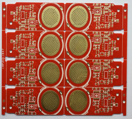
In the traditional design process, PCB design consists of circuit design, layout design, PCB production, measurement and debugging steps in turn. In the circuit design stage, due to the lack of effective methods and means to analyze the transmission characteristics of the signal on the actual PCB board, the circuit design can generally only be carried out based on the suggestions of component manufacturers and experts and past design experience. Therefore, for a new design project, it is usually difficult to make the correct selection of factors such as signal topology and component parameters according to the specific situation.
In the PCB layout design stage, it is also difficult to make real-time analysis and evaluation of the signal performance changes caused by the PCB component layout and signal wiring, so the quality of the layout design depends more on the experience of the designer. In the PCB production stage,

since the processes of each PCB board and component manufacturers are not completely the same, the parameters of the PCB board and components generally have a large tolerance range, making the performance of the PCB board more difficult to control.
In the traditional PCB design process, the performance of the PCB board can be judged by instrument measurement only after the production is completed. The problems found in the PCB board debugging stage must be modified in the next PCB board design. But what is more difficult is that some problems are often difficult to quantify into the parameters in the previous circuit design and layout design. Therefore, for more complex PCB boards, the above-mentioned process usually needs to be repeated many times to finally meet the design requirements.
It can be seen that with the traditional PCB design method, the product development cycle is longer, and the cost of research and development is correspondingly higher.
3. PCB design method based on signal integrity analysis
PCB design process based on signal integrity computer analysis. Compared with the traditional PCB design method, the design method based on signal integrity analysis has the following characteristics:
Before PCB board design, first establish a signal integrity model for high-speed digital signal transmission.
According to the SI model, a series of pre-analysis is carried out on the signal integrity problem, and the appropriate component types, parameters and circuit topology are selected according to the results of the simulation calculation as the basis for circuit design.
In the circuit design process, the design plan is sent to the SI model for signal integrity analysis, and the tolerance range of the components and PCB board parameters, the possible topological structure and parameter changes in the PCB layout design, and other factors are calculated and analyzed. Solution space.
After the circuit design is completed, each high-speed digital signal should have a continuous and achievable solution space. That is, when the PCB and component parameters change within a certain range, the layout of the components on the PCB board and the wiring of the signal lines on the PCB board have a certain degree of flexibility, the requirements for signal integrity can still be guaranteed .
Before the PCB layout design starts, the boundary value of each signal solution space obtained is used as the constraint condition of the layout design, which is used as the design basis for the layout and wiring of the PCB layout.
In the PCB layout design process, the partially completed or fully completed design is sent back to the SI model for post-design signal integrity analysis to confirm whether the actual layout design meets the expected signal integrity requirements. If the simulation results cannot meet the requirements, you need to modify the layout design and even the circuit design, which can reduce the risk of product failure due to improper design.
After the PCB design is completed, the PCB board can be made. The tolerance range of the PCB manufacturing parameters should be within the range of the solution space of the signal integrity analysis.
After the PCB board is manufactured, the instrument is used for measurement and debugging to verify the correctness of the SI model and SI analysis, and use this as the basis for correcting the model.
On the basis of the correct SI model and analysis method, usually the PCB board can be finalized without or only a few repeated modifications to the design and production, which can shorten the product development cycle and reduce the development cost.