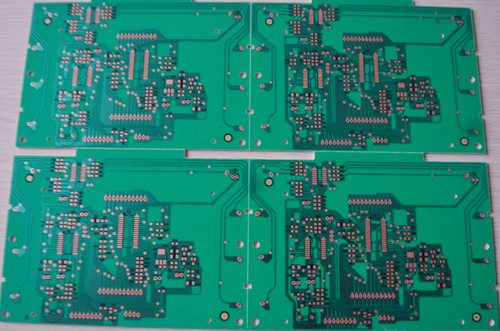
Printed circuit boards (PCB circuit boards), also known as printed circuit boards, are providers of electrical connections for electronic components. Its development has a history of more than 100 years, and its design is mainly layout design. The main advantage of using circuit boards is to greatly reduce wiring and assembly errors, and improve the level of automation and production labor rate. According to the number of layers of the circuit board, it can be divided into single board, double board, four-layer board, six-layer board and other multi-layer circuit boards.
In recent years, China's printed circuit board manufacturing industry has developed rapidly, and its total output value ranks first in the world. With its industrial layout, cost and market advantages, China has become the world's most important printed circuit board production base. Printed circuit boards have developed from single-layer to double-layer, multi-layer, and flexible boards, and continue to develop in the direction of high precision, high density, and high reliability.

The continuous reduction of volume, cost reduction and performance improvement make the printed circuit board still maintain a strong vitality in the development of electronic products in the future. The future development trend of printed circuit board manufacturing technology is to high-density, high-precision, fine pore size, fine wire, small spacing, high reliability, multi-layer, high-speed transmission, light weight, and thin type.
The current PCB circuit board is mainly composed of the following parts
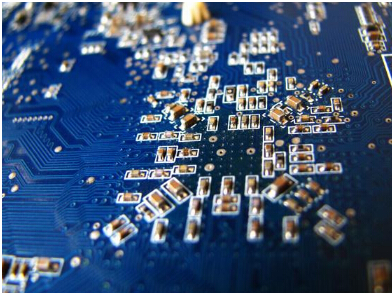
Circuits and drawings: Circuits are tools that conduct electricity between original parts. In addition, a large copper surface will be designed as a ground and power plane. The circuit and drawings are made at the same time.
Dielectric layer: used to maintain the insulation between the line and the layer, commonly known as the substrate.
Through holes: Through holes can open two or more circuits to each other. Larger through holes can be used as part plug-ins. In addition, there are non-through holes (NPTH) that are usually used for surface mounting positioning and fixing screws during assembly.
Soldering ink: not all copper surfaces need to be tin, so the area that does not eat tin will be printed with a layer of material (usually epoxy resin), so that the copper surface does not eat tin and avoids the gap between non-tin-containing wires Short circuit. According to different processes, it is divided into green oil, red oil and blue oil.
Screen: This is an unnecessary structure. The main function is to mark the name and position of each component on the circuit board to facilitate maintenance and identification after assembly.
Due to the repeatability (reproducibility) and consistency of the graphics, the errors of wiring and assembly are reduced, and the maintenance, debugging and inspection time of the equipment is saved.
The design can be standardized to facilitate interchangeability;
It is conducive to mechanized and automated production, improves labor productivity, and reduces the cost of electronic equipment.
In particular, the bending resistance and accuracy of FPC soft boards are better used in high-precision instruments (such as cameras, mobile phones, etc.). Camera, etc.)
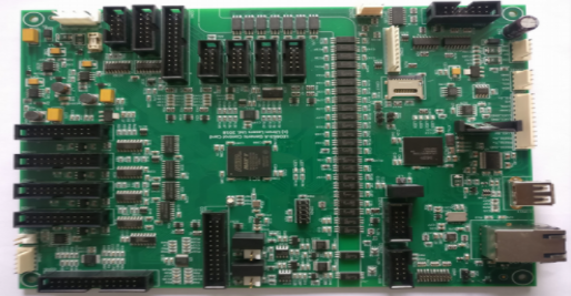
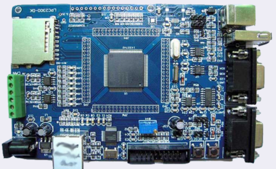
PCB layout is to place circuit components in the wiring area of the printed circuit board. Whether the layout is reasonable not only affects the subsequent wiring work, but also has an important impact on the performance of the entire circuit board. After ensuring the circuit functions and performance indicators, in order to meet the processing performance, inspection and maintenance requirements, PCB components should be uniformly, neatly and compactly placed on the PCB to minimize and shorten the leads and connections between the components, thereby A uniform packing density is obtained.
Arrange the position of each functional circuit unit according to the circuit flow. For input and output signals, the high and low levels should not intersect as much as possible, and the signal transmission line should be the shortest.