Solution:
1. Give the laminate manufacturer a complete list of solvents and solutions used, including the processing time and temperature for each step. Analyze whether copper stress and excessive thermal shock have occurred in the electroplating process.
2. Earnestly comply with the recommended mechanical PCB processing methods. Frequent analysis of metallized holes can control this problem.
3. Most of the pads or wires are detached due to the lack of strict requirements for all operators. If the temperature inspection of the solder bath fails or the residence time in the solder bath is prolonged, detachment will also occur. In the manual soldering repair operation,

the pad detachment is probably caused by the use of improper wattage electric ferrochrome and the failure to conduct professional process training. Now some laminate manufacturers have manufactured laminates with high peel strength levels at high temperatures for strict soldering applications.
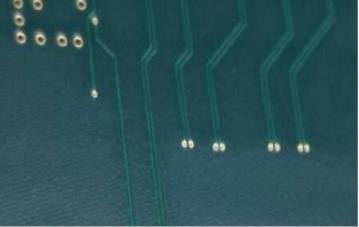
4. If the detachment caused by the design wiring of the printed board occurs in the same place on each board; then the printed board must be redesigned. Usually, this does happen where thick copper foil or wires are at right angles. Sometimes this phenomenon occurs with long wires; this is because of the different coefficients of thermal expansion.
5. Where possible, remove heavy components from the entire printed board or install them after the dip soldering operation. Usually use a low-wattage electric soldering iron to carefully solder, which is shorter than the component dip soldering, the substrate material is heated for a shorter time.
Various soldering problems
Now it is a sign: there are blast holes in cold solder joints or tin solder joints.
Inspection method: Perform frequent analysis of the holes before and after immersion soldering to find the places where the copper is stressed. In addition, carry out incoming inspection of the raw materials.
possible reason:
1. The blast hole or cold solder joint is seen after the soldering operation. In many cases, poor plating, followed by expansion during the soldering operation, resulting in holes or blast holes in the metallized hole wall. If this is produced during the wet PCB processing process, the absorbed volatiles are covered by the coating and then driven out under the heating effect of the dip soldering, which will result in spouts or blast holes.
Solution:
1. Try to eliminate copper stress. The expansion of the laminate in the z-axis or thickness direction is usually related to the material. It can promote the fracture of metallized holes. Deal with laminate manufacturers to get recommendations for materials with less z-swelling.
8. The problem of excessive size change
Now it is a sign: the size of the substrate is out of tolerance or can not be aligned after PCB processing or soldering.
Inspection method: Fully carry out quality control during PCB processing.
possible reason:
1. No attention was paid to the texture direction of the paper-based material, and the expansion in the forward direction is about half of the transverse direction. Moreover, the substrate cannot be restored to its original size after cooling.
2. If the local stress in the laminate is not released, it will sometimes cause irregular dimensional changes during PCB processing.
Solution:
1. Instruct all the production staff to cut the board according to the same texture direction. If the size change exceeds the allowable range, consider switching to a substrate.
2. Contact the laminate manufacturer for advice on how to relieve the material stress before PCB processing.