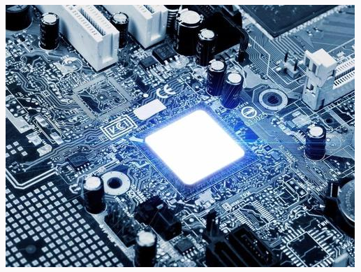
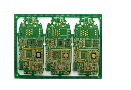
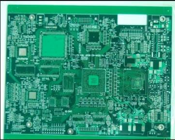
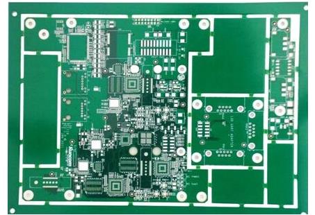
What is a PCB explosion board?
PCB explosion refers to the occurrence of copper foil blistering, substrate blistering, and delamination due to heat or mechanical action during the processing of the PCB; or when the finished PCB is subjected to thermal shock such as immersion soldering, wave soldering or reflow soldering, The occurrence of copper foil blistering, circuit shedding, substrate blistering, delamination, etc. are collectively referred to as bursting.
The cause of the board burst is mainly due to insufficient heat resistance of the substrate, or some problems in the production process, such as high operating temperature or long heating time.
The main reasons for the burst of the copper clad laminate are as follows:
Insufficient curing of substrate
Insufficient curing of the substrate will reduce the heat resistance of the substrate, and the copper clad laminate is prone to bursting when the PCB is processed or subjected to thermal shock. The reason for insufficient curing of the substrate may be the low holding temperature during the lamination process, insufficient holding time, or insufficient amount of curing agent.

When the user responds to the board failure problem, you can first check and solve the board failure method from the following aspects!
1. The substrate absorbs moisture
If the substrate is not well kept in the storage process, the substrate will absorb moisture, and the release of moisture during the PCB board manufacturing process will also easily cause the board to burst. Printed circuit board factories should repackage the copper clad laminates that have not been used up after opening the package to reduce the moisture absorption of the substrate.
For the pressing of multilayer printed circuit boards, after the prepreg is taken out from the cold base, it should be stabilized in the above-mentioned air-conditioned environment for 24 hours before it can be cut and laminated with the inner layer board. After the lamination is completed, it must be sent to the press for compression within one hour to prevent the prepreg from absorbing moisture due to dew point and other factors, causing white corners, bubbles, delamination, and thermal shock of the laminated product. .
After being stacked and fed into the press, the air can be pumped first, and then the press can be closed, which is very good for reducing the impact of moisture on the product.
2. The substrate Tg is low
When using copper clad laminates with relatively low Tg to produce circuit boards with relatively high heat resistance requirements, because the heat resistance of the substrate is low, the problem of board bursting is likely to occur. When the substrate is insufficiently cured, the Tg of the substrate will also be reduced, and it is also prone to bursting or the color of the substrate becoming darker and yellow during the PCB production process. This situation is often encountered in FR-4 products. At this time, it is necessary to consider whether to use a copper clad laminate with a relatively high Tg. In the early production of FR-4 products, only epoxy resin with a Tg of 135°C was used. If the production process is not suitable (such as improper selection of curing agent, insufficient curing agent dosage, low insulation temperature during product lamination, or insufficient insulation time, etc.), the substrate Tg is often only around 130°C. In order to meet the requirements of PCB users, the Tg of general-purpose epoxy resins can reach 140°C. When users report that the PCB manufacturing process has a problem of board burst or the color of the substrate becomes darker and yellow, you can consider using a higher level of Tg epoxy resin.
The above situation is often encountered in composite CEM-1 products. For example, the CEM-1 product has a crack in the PCB process, or the color of the substrate becomes darker and yellow, or "earthworm patterns" appear. This situation is not only related to the heat resistance of the FR-4 bonding sheet on the surface of the CEM-1 product, but also related to the heat resistance of the resin formulation of its paper core material. At this time, efforts should be made to improve the heat resistance of the resin formulation of the CEM-1 product paper core material. After years of research, the author has improved the resin formula of CEM-1 paper core material and increased its heat resistance, greatly improved the heat resistance of composite CEM-1 products, and completely solved the problem of wave soldering and reflow soldering. When the board bursts and discoloration issues.
3. The influence of the ink on the marking material
If the ink printed on the marking material is thicker and it is placed on the surface that is in contact with the copper foil, because the ink is incompatible with the resin, the adhesion of the copper foil may decrease and the problem of plate bursting may occur.
The above three methods can solve the problem of board burst. The PCB production process is basically automatic and mechanized. It is inevitable that problems will occur during the production process. This requires us to strictly control the quality of humans to make qualified PCBs. plate!