PCB board lamination refers to a method in which two or more layers of the same or different materials are combined into a whole by heating and pressing with or without adhesives. This process is very common in China, and is usually used in the production process of multi-layer boards. Today we will take a look at the production process of multi-layer PCB board lamination!
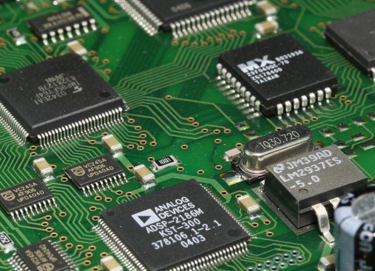
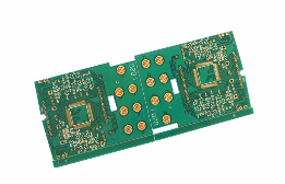
Multi-layer PCB board
After cutting the different raw material blanks according to the specified size, different numbers of blanks are selected according to the thickness of the plate to form a slab, and the stacked slabs are assembled into a pressing unit in order according to the process requirements. Push the pressing unit into the laminator for pressing. The temperature control can be divided into 5 stages:
(a) Preheating stage: the temperature is from room temperature to the starting temperature of the curing reaction of the surface layer, while the core layer resin is heated, and part of the volatiles is discharged, and the applied pressure is 1/3 to 1/2 of the full pressure.
(b) Insulation stage: the surface layer resin is cured at a lower reaction speed. The core layer resin is evenly heated and melted, and the resin layer interfaces begin to fuse with each other.

(c) Heating stage: Raise the temperature from the start of curing to the maximum temperature specified during pressing. The heating speed should not be too fast, otherwise the surface layer will cure too fast, and it will not be well integrated with the core layer resin, resulting in delamination or cracks in the finished product. .
(d) Constant temperature stage: When the temperature reaches the highest value, it remains constant. The function of this stage is to ensure that the surface layer resin is fully cured, the core layer resin is uniformly plasticized, and the fusion bonding between the layers of the material is guaranteed under pressure. Under the action, it becomes a uniform and dense whole, and then the performance of the finished product reaches the best value.
(e) Cooling stage: When the surface layer resin in the slab has been fully solidified and fully fused with the core layer resin, the temperature can be cooled down. The cooling method is to pass cooling water through the hot plate of the press, or it can be natural cool down. This stage should be carried out while maintaining the specified pressure and controlling the appropriate cooling rate. When the temperature of the board drops below the appropriate temperature, the pressure can be unloaded and demoulded.
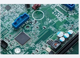
Common failure factors of PCB copy board
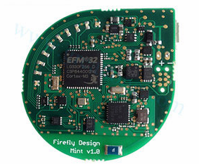
PCB copy board
1. PCB short circuit caused by running tin
1. Improper operation in the de-filming medicine tank causes tin running;
2. Superimposing the unfilmed boards causes tin runaway.
2. PCB short circuit caused by impure etching
1. The quality of the etching potion parameter control directly affects the etching quality.
3. Visible PCB micro short circuit
1. Micro short circuit caused by scratches on Mylar film on the exposure machine;
2. The circuit is slightly short-circuited due to scratches on the glass on the exposure plate.
Four, short circuit of sandwiched PCB
1. The anti-plating film layer is too thin. During electroplating, the plating layer exceeds the film thickness, forming a film, especially the smaller the line spacing, the easier it is to cause the film short circuit.
2. The pattern of the board is not uniformly distributed. During the pattern electroplating process of several isolated lines, the plating layer exceeds the film thickness due to the high potential, forming a sandwich film and causing a short circuit.
Five, invisible PCB micro short circuit
The invisible micro-short circuit is the longest trouble and once the most difficult problem for our company. About 50% of the finished boards that have problems in the test are caused by this type of micro-short circuit. The main reason is the line spacing. There are metal wires or metal particles that are invisible to the naked eye.
Six, fixed position PCB short circuit
The main reason is that the film line is scratched or the coated screen is blocked by garbage, and the fixed position of the coated anti-plating layer is exposed to copper, which causes a short circuit.