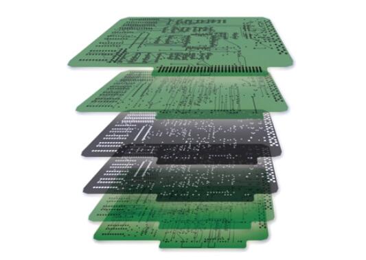
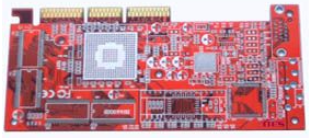
When designing a PCB (printed circuit board), one of the most basic issues that need to be considered is how many wiring layers, ground planes and power planes are needed to achieve the functions required by the circuit, and the wiring layers, ground planes and power supplies of the printed circuit board The determination of the number of layers of the plane is related to requirements such as circuit function, signal integrity, EMI, EMC, and manufacturing cost. For most designs, there are many conflicting requirements in the PCB performance requirements, target cost, manufacturing technology, and system complexity. The PCB laminate design is usually determined by a compromise after considering various factors. High-speed digital circuits and radio circuits usually adopt multi-layer board designs.
The 8 principles that should be paid attention to in cascading design are listed below:
1. Stratification
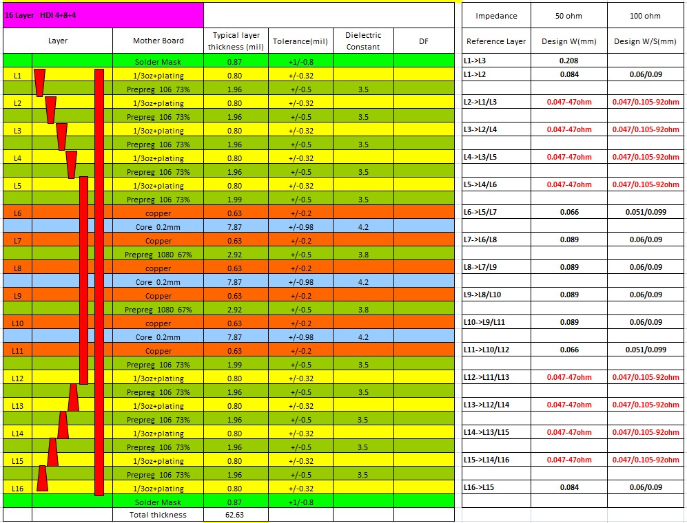
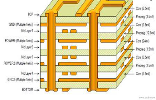
In a multi-layer PCB, it usually contains a signal layer (S), a power (P) plane, and a ground (GND) plane. The power plane and the ground plane are usually solid planes without divisions. They will provide a good low-impedance current return path for the current of the adjacent signal traces. The signal layer is mostly located between these power or ground reference plane layers, forming a symmetrical stripline or an asymmetrical stripline. The top and bottom layers of a multilayer PCB are usually used to place components and a small number of traces. These signal traces must not be too long to reduce the direct radiation generated by the traces.

2. Determine the single power reference plane (power plane)
Using decoupling capacitors is an important measure to solve power integrity. Decoupling capacitors can only be placed on the top and bottom layers of the PCB. The traces, pads, and vias of the decoupling capacitors will seriously affect the effect of the decoupling capacitors. This requires that the traces connecting the decoupling capacitors should be as short and wide as possible when designing, and the wires connected to the vias should also Keep it as short as possible. For example, in a high-speed digital circuit, you can place the decoupling capacitor on the top layer of the PCB, assign the second layer to the high-speed digital circuit (such as a processor) as the power layer, use the third layer as the signal layer, and use the fourth layer as the signal layer. Set as high-speed digital circuit ground.
In addition, try to ensure that the signal traces driven by the same high-speed digital device use the same power layer as the reference plane, and this power layer is the power supply layer of the high-speed digital device.
3. Determine the multi-power reference plane
The multi-power reference plane will be divided into several physical areas with different voltages. If the signal layer is close to the multi-power supply layer, the signal current on the signal layer nearby will encounter an undesirable return path, causing gaps in the return path. For high-speed digital signals, this unreasonable return path design may cause serious problems, so it is required that the high-speed digital signal wiring should be far away from the multi-power reference plane.
4. Determine multiple ground reference planes (ground planes)
Multiple ground reference planes (ground planes) can provide a good low-impedance current return path, which can reduce common-mode EMl. The ground plane and power plane should be tightly coupled, and the signal layer should also be tightly coupled with the adjacent reference plane. This can be achieved by reducing the thickness of the medium between layers.
5. Reasonably design the wiring combination
The two layers spanned by a signal path are called a "wiring combination." The best wiring combination design is to avoid the return current from flowing from one reference plane to another, but from one point (surface) of a reference plane to another point (surface). In order to complete complex wiring, the layer-to-layer conversion of traces is inevitable. When switching between signal layers, ensure that the return current can flow smoothly from one reference plane to another. In a design, it is reasonable to use adjacent layers as a wiring combination. If a signal path needs to span multiple layers, it is usually not a reasonable design to use it as a wiring combination, because a path through multiple layers is not smooth for the return current. Although it is possible to reduce ground bounce by placing decoupling capacitors near the vias or reducing the thickness of the dielectric between the reference planes, it is not a good design.
6. Set the wiring direction
On the same signal layer, it should be ensured that most of the wiring directions are consistent, and should be orthogonal to the wiring direction of adjacent signal layers. For example, the wiring direction of one signal layer may be set as the "Y-axis" direction, and the wiring direction of another adjacent signal layer may be set as the "X-axis" direction.
7. Adopt even-numbered layer structure
It can be found from the designed PCB stack that almost all the classic stack designs are even-numbered layers, not odd-numbered layers. This emergency is caused by many factors, as shown below.
It can be understood from the manufacturing process of the printed circuit board that all the conductive layers in the circuit board are saved on the core layer. The material of the core layer is generally a double-sided superstrate. When the core layer is fully utilized, the conductive layer of the printed circuit board The number is even.
Even-numbered printed circuit boards have cost advantages. Due to the lack of a layer of dielectric and copper, the raw material cost of the odd-numbered printed circuit board is slightly lower than the cost of the even-numbered printed circuit board. However, because odd-numbered printed circuit boards need to add a non-standard laminated core layer bonding process on the basis of the core layer structure process, the processing cost of odd-numbered printed circuit boards is significantly higher than that of even-numbered printed circuit boards. Compared with the ordinary core layer structure, adding copper to the core layer structure will result in a decrease in production efficiency and a prolonged production cycle. Before lamination and bonding, the outer core layer needs additional processing, which increases the risk of scratches and wrong etching of the outer layer. The additional outer layer treatment will greatly increase the manufacturing cost.
When the printed circuit board is in the multilayer circuit bonding process, when the inner and outer layers are cooled, different lamination tensions will cause the printed circuit board to bend to different degrees. Moreover, as the thickness of the circuit board increases, the risk of bending of the composite printed circuit board with two different structures becomes greater. Odd-numbered circuit boards are easy to bend, and even-numbered printed circuit boards can avoid circuit board bending.
When designing, if an odd number of layers are stacked, the following method can be used to increase the number of layers.
If the power supply layer of the design printed circuit board is an even number and the signal layer is an odd number, the method of adding a signal layer can be adopted. The added signal layer will not lead to an increase in cost, but can shorten the processing time and improve the quality of the printed circuit board.
If you design the printed circuit board with an odd number of power layers and an even number of signal layers, you can use the method of adding a power layer. And another simple method is to add a ground layer in the middle of the stack without changing other settings, that is, to route the printed circuit board on an odd-numbered layer first, and then copy a ground layer in the middle.
In microwave circuits and mixed media (different dielectric constants) circuits, a blank signal layer can be added near the center of the printed circuit board stack to minimize stack imbalance.
8. Cost considerations
In terms of manufacturing cost, with the same PCB area, the cost of a multi-layer circuit board is definitely higher than that of a single-layer and double-layer circuit board, and the more layers, the higher the cost. But when considering the realization of circuit functions and circuit board miniaturization, and ensuring signal integrity, EMl, EMC and other performance indicators, multi-layer circuit boards should be used as much as possible. Comprehensive evaluation, the cost difference between multi-layer circuit boards and single-layer circuit boards will not be much higher than expected.