One, the process of soldering the heating bridge in the smt patch processing plant is not appropriate. The soldering thermal bridge in the SMT patch prevents the solder from forming a bridge. If this process is not operated properly, it will cause cold solder joints or insufficient solder flow. Therefore, the correct soldering habit should be to place the soldering iron tip between the pad and the pin, and the tin wire is close to the soldering iron tip. When the tin melts, move the tin wire to the opposite side, or place the solder wire between the pad and the pin., The soldering iron is placed on the tin wire, and the tin wire is moved to the opposite side when the tin is melted; in this way, a good solder joint can be produced and the chip processing will not be affected.
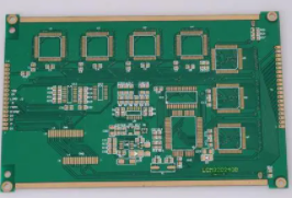
Smt patch processing plant
2. Excessive force is applied to the lead welding during SMT patch processing. Many SMT workers believe that too much force can promote the heat conduction of the solder paste and promote the soldering effect, so they are used to pressing down forcefully during soldering. In fact, this is a bad habit, which can easily cause problems such as warping, delamination, depression, and white spots on the PCB of the patch.

Therefore, it is completely unnecessary to use excessive force during the soldering process. In order to ensure the quality of the patch processing, it is necessary to gently touch the PCB soldering iron tip to the pad.
3. Randomly choose the soldering iron tip, regardless of the suitable size. In the process of patch processing, the size of the soldering iron tip is very important. If the size of the soldering iron tip is too small, it will extend the residence time of the soldering iron tip and cause insufficient solder flow and lead to cold solder joints. If the size of the soldering iron tip is too large, the joint will heat up too quickly and burn the patch. Therefore, the selection of the suitable soldering iron tip size should be based on the three criteria of the correct length and shape, the correct heat capacity, and the larger the contact surface but slightly smaller than the pad.
4. The temperature setting is incorrect. Temperature is also an important factor in the soldering process. If the temperature is set too high, it will cause the pad to lift, the solder will be overheated and the circuit patch will be damaged. Therefore, setting the correct temperature is particularly important for the quality assurance of patch processing.
5. Improper use of flux. It is understood that many workers are accustomed to using too much flux in the process of patch processing. In fact, this will not only not help you to have a good solder joint, but it will also cause the problem of whether the lower solder joint is reliable or not, which is easy to produce. Corrosion, electron transfer and other issues.
6. Improper transfer welding operation. Transfer soldering refers to adding solder to the tip of the soldering iron first, and then transfer to the connection. Inappropriate transfer soldering will damage the tip of the soldering iron and cause poor wetting. Therefore, the normal transfer soldering method should be that the soldering iron tip is placed between the pad and the pin, the soldering wire is close to the soldering iron tip, and the soldering wire is moved to the opposite side when the tin is melted. Place the tin wire between the pad and the pin. Place the soldering iron on the tin wire and move the tin wire to the opposite side when the tin melts.
7. Unnecessary modification or rework. The bigger taboo in the soldering process of patch processing is to modify or rework in pursuit of perfection. This approach not only fails to make the quality of the patch perfect, on the contrary, it is easy to cause the metal layer of the patch to break and the PCB board to delaminate, waste unnecessary time and even cause scrap. So don't do unnecessary modification and rework on the patch.