Is there any way for SMT patch to reduce some failure problems?
SMT patch refers to the abbreviation of a series of technological processes that are processed on the basis of PCB. PCB (Printed Circuit Board) is a printed circuit board. So, is there any way for SMT patch to reduce some failure problems?
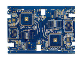
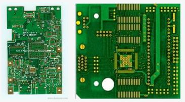
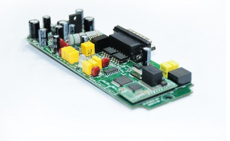
SMT patch
The manufacturing process, handling, and printed circuit assembly (PCA) testing all subject the package to a lot of mechanical stress, which can cause failure. As the grid array package becomes larger and larger, how to set the security level for these steps becomes more and more difficult.
For many years, the monotonic bending point test method is a typical feature of the package. The test is described in IPC/JEDEC-9702 "Monotonic Bending Characteristics of Board Level Interconnects". This test method describes the breaking strength of the horizontal interconnection of printed circuit boards under bending load.

However, this test method cannot determine the maximum allowable tension.
For the manufacturing process and assembly process, especially for lead-free PCA, one of the challenges it faces is the inability to directly measure the stress on the solder joints. The most widely used metric used to describe the risk of interconnected components is the tension of the PCB printed circuit board adjacent to the component, which is described in IPC/JEDEC-9704 "Printed Wiring Board Strain Test Guidelines".
A few years ago, Intel realized this problem and began to develop a different testing strategy to reproduce the worst bending situation in practice. Other companies such as Hewlett-Packard also realized the benefits of other testing methods and began to consider similar ideas to Intel. As more and more chip manufacturers and customers realize that the determination of the tension limit used to minimize mechanical failures during manufacturing, handling and testing is of great value, this method has caused more and more attentions. interest.
As the use of lead-free equipment expands, users are more and more interested; because many users are facing quality problems.
With the increase of interest from all parties, IPC feels it is necessary to help other companies develop various test methods that can ensure that BGAs are not damaged during manufacturing and testing. This work is jointly carried out by the IPC 6-10d SMT Attachment Reliability Test Method Working Group and the JEDEC JC-14.1 Packaged Equipment Reliability Test Method Subcommittee, and the work has been completed.
The test method specifies eight contact points arranged in a circular array. The PCA with a BGA installed in the center of the PCB printed circuit board is placed in this way: the component is mounted face down on the support pins, and the load is applied to the back of the BGA. Place the strain gauge adjacent to the part according to the recommended gauge layout of IPC/JEDEC-9704.
The PCA will be bent to the relevant tension level, and the failure analysis can determine the degree of damage caused by the deflection to these tension levels. The iterative method can be used to determine the level of tension that does not cause damage. This is the tension limit.