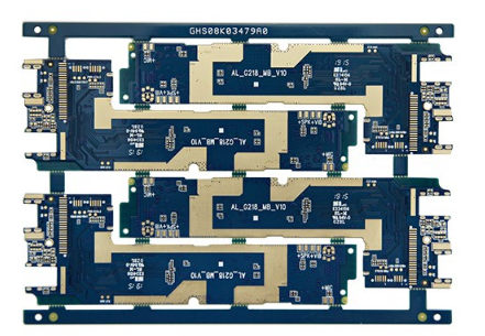
In the high-speed PCB design and wiring, line length matching is generally required. At this time, it is necessary to set constraint rules and assign these rules to various net groups. The following takes ddr as an example to illustrate the specific steps of setting these constraints.
1. PCB design and wiring requirements
DDR clock: line width 10mil, internal spacing 5mil, external spacing 30mil. Differential PCB design and wiring are required, and the differential pair wiring error must be accurately matched, allowing within +20mil
DDR address, chip select and other control lines: line width 5mil, internal spacing 15mil, external spacing 20mil, should be in a daisy chain topology, which can be 1000-2500mil longer than the ddrclk line, and must not be shorter

DDR data lines, ddrdqs, ddrdm lines: line width 5mil, internal spacing 15mil, external spacing 20mil, it is best to design and route on the same layer of PCB. The line length difference between the data line and the clock line is controlled within 50mil.
2. According to the above requirements, set different constraints in PCB design Allegro
For the line width (physical), only 3 constraints need to be set: DDR_CLK, DDR_ADDR, DDR_DATA
After setting the above constraints, you can add these constraints to the net. Click attach... in the physical rule set, and then click more in the control panel on the right,
pop-up dialogue box
Find ckn0 and ckp0, click apply, it will pop up
Select NET_PHYSICAL_TYPE in the list on the left, enter DDR_CLK in the space on the right, and click apply to pop up
That is, the two nets have added the NET_PHYSICAL_TYPE attribute, and the value is DDR_CLK.
Similarly, you can set the NET_PHYSICAL_TYPE of the DDR data line, the data strobe line and the data shield line to DDR_DATA, and the NET_PHYSICAL_TYPE of the DDR address line, chip select line, and other control lines to DDR_ADDR.
After the above steps are completed, the constraints that have been set must be assigned to these net groups.
Click assignment table...
pop-up dialogue box
Choose their own physical constraints for different signal groups
Someone may ask, why are there area0 and area1? This is because these constraints are impossible to achieve in some places. For example, in the cpu of the bga package, when the leads come out, the line spacing cannot reach 30, 20 or even 10 mils. In these places, if you follow this constraint, it is impossible to eliminate the drc in the PCB. At this time, a solution is to classify these places as a room, and then add the room attribute to it (that is, the name of the room area0, 1, etc.). For these rooms, set appropriate constraints (ibid.).
Regarding the line spacing, since each is divided into the spacing within the group and the spacing outside the group, there are 6 constraints in total:
DDR_CLK_INNER,DDR_CLK_OUTER,…………………………
Just set the line to line and line to shape for these six constraints, and set them according to the above requirements respectively.
The remaining steps are the same as the settings in physical. But at this time the assignment table becomes the following.
The above is the detailed content about the setting steps of Allegro constraint rules for PCB design.