Even if the wiring in the entire PCB board is completed very well, the interference caused by the improper consideration of the power supply and the ground wire will reduce the performance of the product, and sometimes even affect the success rate of the product. Therefore, the wiring of the electric and ground wires must be taken seriously, and the noise interference generated by the electric and ground wires should be minimized to ensure the quality of the product.
Every engineer engaged in the design of electronic products understands the cause of the noise between the ground wire and the power wire, and now only the reduced noise suppression is described:

It is well known to add decoupling capacitors between the power supply and ground.
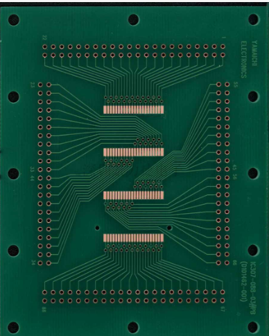
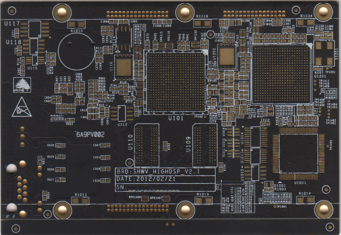
Widen the width of the power and ground wires as much as possible, preferably the ground wire is wider than the power wire, their relationship is: ground wire>power wire>signal wire, usually the signal wire width is: 0.2~0.3mm, the smallest width can be reached 0.05~0.07mm, power cord is 1.2~2.5 mm
For the PCB of the digital circuit, a wide ground wire can be used to form a loop, that is, to form a ground net for use (the ground of the analog circuit cannot be used in this way). A large area of copper layer is used as a ground wire, which is not used on the printed circuit board. The above places are connected to the ground as a ground wire. Or it can be made into a multilayer board, and the power supply and ground wires occupy one layer each.
2. Common ground processing of digital circuit and analog circuit
Nowadays, many PCBs are no longer single-function circuits (digital or analog circuits), but are composed of a mixture of digital and analog circuits. Therefore, it is necessary to consider the mutual interference between them when wiring, especially the noise interference on the ground wire.
The frequency of the digital circuit is high, and the sensitivity of the analog circuit is strong. For the signal line, the high-frequency signal line should be as far away as possible from the sensitive analog circuit device. For the ground line, the whole PCB has only one node to the outside world, so The problem of digital and analog common ground must be dealt with inside the PCB, and the digital ground and analog ground inside the board are actually separated, they are not connected to each other, but at the interface (such as plugs, etc.) connecting the PCB to the outside world. There is a short connection between the digital ground and the analog ground. Please note that there is only one connection point. There are also non-common grounds on the PCB, which is determined by the system design.
3. The signal line is laid on the electric (ground) layer
When wiring multi-layer printed circuit boards, since there are not many wires left in the signal line layer that have not been laid out, adding more layers will cause waste and increase a certain amount of work in production, and the cost will increase accordingly. To solve this contradiction, you can consider wiring on the electrical (ground) layer. The power layer should be considered first, and the ground layer second. Because it is best to preserve the integrity of the formation.