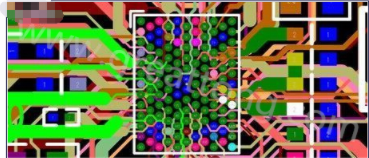
PCB size
The microcontroller is Silicon Labs' EFM8 Sleepy Bee, and the (relative) large connector on the left provides a direct connection to the SiLabs USB debug adapter. This connector consumes quite a bit of PCB space, making the overall design appear larger than it really is.
The figure below shows the PCB board dimensions in inches. The shorter horizontal size is my attempt to estimate how small the board could be if the debug connector were removed (and other components rearranged).

Here are some other ways to reduce the size of the board:
. I chose the larger passive components IC (0805 and 1206) because they are easier to assemble. If you plan to assemble boards, you might consider using an 0603 or even an 0402 (you may find acceptable 2.2μF capacitors in an 0402 package, but for 0.1μF capacitors and resistors, you can use an 0402).
. I chose a larger package for the microcontroller; This is a 9mm x 9mm QFP32. The 32-pin pinless package size is significantly smaller (5 mm x 5 mm), and there is a 24-pin pinless package size that is even smaller (4 mm x 4 mm). In my opinion, most applications built around this power supply do not require more than a few I/O pins, so a 24-pin package is probably the best choice. I used the 32-pin device because the microcontroller does not have any other lead (i.e., non-lead) package.
. I provide 32.768khz crystal oscillator for real-time clock applications; It is about the size of an 0805 component. The microcontroller has an internal low-power oscillator with a very low degree (± 10%), so if you don't need timing, you can omit the crystal.
. Charge pump switch regulators currently have four 2.2μF output capacitors, but only one is required.
. LED and its resistance is only used for debugging; They can be omitted from the final design.
. You may think that you can eliminate all the circuits (switches, LDO, and two capacitors) associated with debugging power supplies. I don't recommend this because solar power is not a convenient source for firmware development and testing.
Double choice
The latter item on how to make a smaller list is to have components at the top and bottom of the board. As I was writing this ARTICLE, I began to wonder if the entire circuit would fit in the area corresponding to the size of the solar cell, so that you could design a circuit board that just had the solar cell on top and everything else on the bottom. I decided to remove some unnecessary components from the schematic and try this idea, and here's what I found (in inches) :
It's a rough approximation, but, as you can see, we're pretty close to cramming all the circuits into the PCB space that the solar cells take up.
To create this component placement, I eliminated three of the four output capacitors, the crystal, the LED, and the RESISTANCE of the LED. I also switched the microcontroller package to QFN24. The passive components are still 1206 and 0805, but these larger packages can compensate for the need for some way to connect the microcontroller to the debug adapter. There's certainly not a lot of routing space, but if you can use a four-ply board (and still have plenty of room at the top below the solar cell), I don't think this is a serious hurdle.
Conclusion
We have discussed the PCB layout of my recently designed solar microcontroller board, and we have also studied an example of a more spatially optimized implementation where the PCB size is close to the size of a solar cell. If you have any experience with space-constrained designs for low-power embedded devices, feel free to share your thoughts in the comments.