One, the type of circuit board proofing
The development of circuit board technology has played a crucial role in the rapid development of electronic products.
circuit board proofing single-sided board
We just mentioned that on the most basic PCB, the parts are concentrated on one side, and the wires are concentrated on the other side. Because the wires only appear on one side, we call this type of PCB a single-sided. Because single-sided boards have many strict restrictions on the design of the circuit (because there is only one side, the wiring can not be crossed * and must be a separate path), so only early circuits use this type of board. There are wiring on both sides of the double-sided circuit board. However, to use wires on both sides, there must be a proper circuit connection between the two sides. This kind of "bridge" between circuits is called a via. The pilot hole is a small hole filled or coated with metal on the PCB, which can be connected with the wires on both sides. Because the area of the double panel is twice as large as that of the single panel, and because the wiring can be interleaved (it can be wound to the other side), it is more suitable for use in circuits that are more complicated than the single panel.
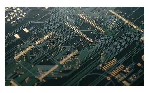
circuit board proofing multilayer board
Vias: There are metal vias and non-metal vias, among which metal vias are used to connect component pins between layers.
Mounting hole: used to fix the circuit board.

Wire: The copper film of the electrical network used to connect the pins of the components.
Connectors: used to connect components between circuit boards.
Filling: used for copper coating of the ground wire network, which can effectively reduce the impedance.
Electrical boundary: used to determine the size of the circuit board, all components on the circuit board cannot exceed the boundary.
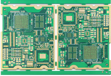
Two, the key points of PCB circuit board design
PCB circuit board is the basic electronic component of all electronic circuit design, as the main support body, it carries all the components that make up the circuit.
1. There must be a reasonable direction
Such as input/output, AC/DC, strong/weak signal, high frequency/low frequency, high voltage/low voltage, etc. Their direction should be linear (or separated), and they should not blend with each other. Its purpose is to prevent mutual interference. The best trend is in a straight line, but it is generally not easy to achieve. The most unfavorable trend is a circle. Fortunately, isolation can be set to improve. For DC, small signal, low voltage PCB board design requirements can be lower. So "reasonable" is relative.
2, choose a good grounding point: the grounding point is often the most important
A small grounding point, I don’t know how many engineers and technicians have talked about it, which shows its importance. Under normal circumstances, a common ground is required, such as: multiple ground wires of the forward amplifier should be merged and then connected to the main ground, and so on. In reality, it is difficult to achieve this completely due to various restrictions, but we should try our best to follow it. This problem is quite flexible in practice. Everyone has their own set of solutions. It is easy to understand if they can explain it for a specific circuit board.
3. Reasonably arrange power filter/decoupling capacitors
Generally, only a number of power filter/decoupling capacitors are drawn in the schematic diagram, but it is not pointed out where they should be connected. In fact, these capacitors are set up for switching devices (gate circuits) or other components that require filtering/decoupling. These capacitors should be placed as close as possible to these components. If they are too far away, they will have no effect. Interestingly, when the power supply filter/decoupling capacitors are arranged properly, the problem of the grounding point becomes less obvious.