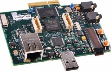
When the PCB design is completed, we all need to perform functional inspections on all items. Just like when we finish the examination papers ourselves, we need to do a simple analysis and check all the questions again to ensure that no major mistakes will be made due to negligence. Similarly, PCB design is the same. The following are the inspection items that need to be carried out after PCB design:
1. DFM review of the light board: Whether the light board production meets the process requirements of PCB manufacturing, including wire width, spacing, wiring, layout, vias, Mark, wave soldering component direction, etc.
2. Review the match between the actual components and the pads: whether the purchased actual SMT components and the designed pads are consistent (if inconsistencies are indicated with a red mark), and whether they meet the minimum spacing requirements of the placement machine.
3. Generate three-dimensional graphics: generate three-dimensional graphics, check whether the space components interfere with each other, whether the component layout is reasonable, is conducive to heat dissipation, whether it is conducive to the heat absorption of SMT reflow welding, etc.

4. Optimization of PCBA production line: optimize placement sequence and material station location. Input the existing placement machine (such as Siemens high-speed machine, global multifunction machine) into the software, and allocate the components on the existing board, how many types Siemens pastes, which locations, how many types around the world, and which ones Location, where to pick up the material, etc. So as to optimize the SMT patch processing program and save time. For multi-line production, the placement of components can also be optimized.
5. Work instructions: automatically generate work instructions for workers on the production line.
6. Revision of inspection rules: The inspection rules can be modified. For example, the minimum component spacing is 0.1mm, which can be set to 0.2mm according to the specific model, manufacturer, and board complexity: the minimum wire width is 6mi, and it can be changed to 5mil for high-density design.
7. Support Panasonic, Fuji, Universal placement software: it can automatically generate placement software, saving programming time.
8. Automatically generate steel plate optimization graphics.
9. Automatically generate AOI and X-RAY programs.
10. Inspection report.
11. Support various software formats (Japan, US KATENCE, China PROTEL).
12. Review the BOM and correct the corresponding errors, such as the manufacturer's spelling errors. And convert the BOM table into software format.
The manufacturing process of double-sided PCB
Double-sided copper clad laminate blanking composite board CNC drilling through hole inspection, deburring brush, chemical plating through hole, metallization, full plate electroplating, thin copper inspection and cleaning, screen printing negative circuit pattern, curing dry film or wet film, exposure, developing inspection and repair Circuit pattern electroplating tin plating anticorrosive nickel gold removal printing material photosensitive film etching copper tin removal and cleaning brush a layer of thermal curing green oil screen printing solder mask pattern photosensitive dry film or wet film, exposure and development heat curing ordinary photosensitive heat curing and oil Record-clean and dry screen printing mark character graphics curing-spray tin or organic solder mask shape treatment clean and dry electrical switch test packaging inspection finished product delivery
As products have higher and higher requirements for functions, ordinary single panels are no longer sufficient to meet the needs of functionalization. What emerged at the historic moment is the double-sided printed PCB circuit board. It means that there are conductive lines on both sides of the circuit board. It is usually made of epoxy glass cloth copper clad laminate. Used in the fields of communication electronic equipment, advanced instruments and meters, high-performance electronic computers, etc. The typical process for manufacturing double-sided plated-hole printed boards is the bare copper-clad solder mask process (SMOBC). The process is as follows:
Double-sided copper clad laminate blanking - composite board CNC drilling through hole inspection, deburring, brush electroless plating (through hole metallization) - (full board electroplating of thin copper) - inspection and cleaning of screen printing negative circuit patterns, curing (dry Film or wet film, exposure, development)-Check and repair circuit pattern plating-Plating tin (anticorrosive nickel/gold)-Remove printing material (photosensitive film)-Etching copper-(Removing tin) and cleaning brush a layer of thermal curing green oil wire Screen printing solder mask pattern (photosensitive dry film or wet film, exposure, development, heat curing, ordinary photosensitive heat) curing and oil recording)-cleaning, drying screen printing marking character graphics, curing-(spray tin or organic solder mask Mold)-shape processing clean, dry, electrical switch test, packaging inspection, finished product delivery.
More multi-layer PCB boards are actually manufactured like this. There are one or two more processes in some links, from printed circuit board manufacturing, component procurement, SMT patch, assembly and testing. It can be done.