So, are you all ready to design your first PCB prototype? We believe this must be a surprise moment for you. We thank you for your eagerness to innovate and try things out of the box. However, if you are confused about further designing your PCB prototype on a low-cost PCB, then this article is for you!
Here, we will give you an in-depth understanding of PCB prototyping. Whether you are a novice or an expert engineer, I believe these steps will benefit you endlessly.
let's start.
Why printed circuit board cost is an important criterion
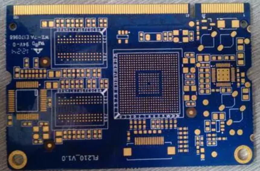
The cost of your printed circuit board is an important criterion. The higher the cost, the more expensive your final product. As a matter of fact, circuit boards can cost anywhere from 50 cents to $300, and can go higher depending on the complexity, number of layers, and installation you plant on them.
aspect
If you want to reduce the cost of the PCB prototype as much as possible, you must control its size. It is foreseeable that the price of PCB will increase as its surface area increases.
Similarly, compared with the traditional form, the design cost of the irregularly shaped PCB board is higher. Because a lot of waste is generated in the manufacturing process.

Number of layers
In fact, the higher the number of layers in the PCB; the greater its complexity. The more complex the PCB design, the higher the cost of the entire process.
Therefore, it is strongly recommended to limit the number of layers as much as possible. A better method here is to stack additional PCB copper layers on top of each other in the form of a highway. They will provide a new plane for electronic routing and serve this purpose well.
Material
If you want to reduce the cost of PCB prototyping as much as possible, you must pay attention to its material type. The standard PCB is made of copper. Other accessible PCB materials used include glass epoxy, also known as FR-4. Here, FR stands for flame retardant, and the previous number stands for its flammability.
FR-4 is the default choice for most PCB manufacturers. However, when designing dielectric constant and material thickness are critical to high-speed board parameters, care must be taken.
Electroplating treatment
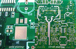
Through the pad electroplating process, the exposed copper surface of the PCB is covered by another metal material. This is to improve the solderability of the pad during assembly. Two standard technologies include HASL and ENIG. If you want low-cost PCB prototyping, you must stick to HASL because ENIG is very expensive.
Board thickness
The thickness of the PCB also plays a vital role in determining the cost of PCB manufacturing. The 1.6mm depth seems to be the industry standard, but it may increase depending on the number of copper layers.
Thick plates determine your production costs. In modern technology, thick plates are expensive, but their functions are not very comprehensive. On the contrary, it is a thinner board that can be used in mobile phones and electronic products. When designing a PCB, you must determine the thickness of the PCB you need, and then develop it. Avoid some problems.
Impedance control
If you plan to integrate Bluetooth, Wi-Fi, and related technologies on the PCB, you must define the impedance accordingly.
PCB impedance depends on many factors, including trace width, prepreg material, and solder mask. Proper impedance control must be performed to optimize wireless antenna performance.
However, since most manufacturers will not provide you with controlled impedance, this will be an additional cost.
Hole size
It is important to determine the correct hole size on the PCB. The holes help establish vertical electrical connections between the copper layers. Although small pads can help you save space (and thus cost), it can make the manufacturer's process difficult.
In addition, a hole that is too small also means a smaller tolerance and may produce more waste, which will cost you more.
Here, the best way is to maintain a balance and choose a hole in the range of 0.2 – 0.3 mm.
Solder mask
Apply a layer of paint-like polymer on the copper traces of the PCB. It prevents the formation of solder bridges and eliminates the possibility of any short circuits.
There is no doubt that the solder mask is essential. If you need to design a low-cost PCB, we can only choose the type and printing method of the solder mask.
There are many types of PCB solder resists, such as:
1. Epoxy liquid
2. Liquid photosensitive imaging
3. Dry film photosensitive imaging
4. Top and bottom masks
It can be selected according to the specific design of the PCB function. If you need special help, you can contact us, we will be happy to provide services to choose the most suitable for you.
Adhere to industry standard sizes
If reducing costs as much as possible is one of the main motivations behind PCB prototyping, it recommends avoiding reinventing the wheel. Stick to industry standard sizes as much as possible.
Because most manufacturers follow the industry scale of these standards, and if you need anything out of the box, their equipment will be tailored to these requirements, and the manufacturer will have to make extra efforts. In turn, it will adversely affect the cost of custom PCBs.
Core component selection
For efficient prototyping, you must have a clear understanding of all the electronic components (such as sensors, microchips, displays, sensors, and connectors) that you want to deploy. The target price of the final product will also play an important role.
The best approach here is to create a relevant block diagram to ensure as much detail as possible and natural continuity.
You can use PCB design software for preliminary design and have the initial documentation of the PCB layout. In this way, some PCBA calculators can be used to calculate the cost in time.
Circuit design
Once you have a basic understanding of what is needed and other expectations, you can create a design schematic. You can simplify this task with the help of designing applications. This diagram will also give you a deeper understanding of how the different components are connected.
Once you have designed a preliminary schematic, please contact us through the website, we can provide you with all the information you want to know about this board.
Low cost PCB-bill of materials
Once the PCB is manufactured, layout failures are likely to occur, which will have a negative impact on the functionality of the final product. Several PCB layouts have been completed, and now is a good time to generate a bill of materials. It can be automatically created by schematic design software. The proposal includes part numbers, quantities, and other specifications.
You can then analyze the bill and see which are the most expensive for future analysis and improvement.
Low cost PCB-experiment and repeat
Retrieve the PCB from the manufacturer and evaluate it correctly. It is possible that your PCB may not meet your requirements. Don't be surprised. Things often do not go as expected.
You must thoroughly weigh the choice and the time it takes to debug on the PCB.
This part may cost you a lot of time, but I think it is worth it because you can find problems and solve them. This is related to the function of making PCB.
in conclusion
How to design a low-cost PCB prototype. The key here is to adhere to industry standards and follow best practices to keep printed circuit board costs to a minimum.
In addition, your PCB manufacturer also plays an important role. Choose to accept the prototype order wholeheartedly and the price is reasonable. They must also provide discounts and be equipped with the right tools to simplify manufacturing.