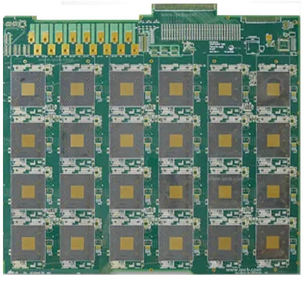
According to the current process capability of domestic circuit board manufacturers, our company temporarily organizes some specifications for PCB board design, please refer to them as appropriate, and follow this rule in the design and production, so as to avoid some parameters that are not suitable for production after the design is completed, which may cause the design to be changed again. Trouble: one
According to the current process capability of domestic circuit board manufacturers, our company temporarily organizes some specifications for PCB board design, please refer to them as appropriate, and follow this rule in the design and production, so as to avoid some parameters that are not suitable for production after the design is completed, which may cause the design to be changed again. trouble:
1. Ordinary single-panel safety distance design:

1: The minimum line width of 1/2oz is 0.1mm, and the minimum line spacing is 0.15mm.
2: The minimum line width of 1oz copper thickness is 0.15mm, and the minimum spacing is 0.15mm.
3: The minimum line width of 2oz copper thickness is 0.25mm, and the minimum spacing is 0.2mm.
Hole and land width:
1: Die punching plate, the smallest hole diameter is greater than 0.65mm. The minimum diameter of CNC shape can be 0.2mm. The tolerance is about 0.05mm.
2: The minimum welding ring of 1oz board should be above 0.1mm. 2oz try to make a ring above 0.25mm.
3: The distance between the smallest pad and the pad should be 0.2mm or more.
4: The distance between the copper foil and the edge of the board should be greater than 0.3mm.
5:1oz cold-proof wound is greater than the minimum value of 0.15mm on one side of the pad, and 2oz should be above 0.2mm.
6: The Vcut test line must be marked when opening the mold, and the Vcut line must be at least 0.3 distance from the line.
7: The size of the v-cut point from the edge of the board should be greater than 0.3mm. The depth is generally about 1/3 of thedepth is the best .
Distance of carbon ink circuit board:
1: Carbon ink should remain 0.3mm without copper. In the case of copper skin, it should be greater than 0.5mm.
2: The carbon ink spacing should be more than 0.3mm.
3: The width of carbon ink is 0.15mm or more larger than that of one side of copper foil.