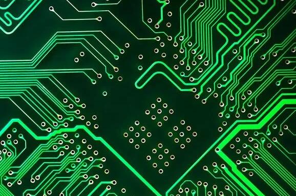
PCB single and double panel laminated design description
Next, the editor of the PCB manufacturer wants to talk to you about some basic operations of PCB stack design; in terms of manufacturing cost, if the PCB area is the same, the cost of a multi-layer circuit board will be more than that of a single Layers and double-layer circuit boards are high, and as the number of layers increases, the cost continues to increase. In PCB design, if an odd number of layers are stacked, the following method can be used to increase the number of layers.
If the power supply layer of the design printed circuit board is an even number and the signal layer is an odd number, the method of adding a signal layer can be adopted. The added signal layer will not lead to an increase in cost, but can shorten the processing time and improve the quality of the printed circuit board.

2. If the power supply layer of the design printed circuit board is odd and the signal layer is even, the method of increasing the power supply layer can be adopted. And another simple method is to add a grounding layer in the middle of the stack without changing other settings, that is, to route the printed circuit board on an odd-numbered layer first, and then copy a grounding layer in the middle.
3. In microwave circuits and mixed media, when it comes to this, do you remember that the media have different dielectric constants? In the circuit, you can add a blank signal layer near the center of the printed circuit board stack to minimize it The effect of stacking imbalance.
There are many things to refer to as to how to choose how many layers of boards are used in the design and what method of stacking to use, such as the density of the components on the circuit board, the PIN density, the frequency of the signal, the size of the board and many other factors to judge. We must consider these factors comprehensively. For the more signal networks, the greater the device density, the greater the PIN density, and the higher the signal frequency, the multilayer board design should be used as much as possible. ipcb is a high-precision, high-quality PCB manufacturer, such as: isola 370hr PCB, high-frequency PCB, high-speed PCB, ic substrate, ic test board, impedance PCB, HDI PCB, Rigid-Flex PCB, buried blind PCB, advanced PCB, microwave PCB, telfon PCB and other ipcb are good at PCB manufacturing. ipcb PCB has always been responsible for satisfying customer needs. iPCB is happy to be your business partner. Our business goal is to become the most professional prototyping PCB manufacturer in the world. Mainly focus on microwave high frequency PCB, high frequency mixed pressure, ultra-high multi-layer IC testing, from 1+ to 6+ HDI, Anylayer HDI, IC Substrate, IC test board, rigid flexible PCB, ordinary multi-layer FR4 PCB, etc. Products are widely used in industry 4.0, communications, industrial control, digital, power, computers, automobiles, medical, aerospace, instrumentation, Internet of Things and other fields.