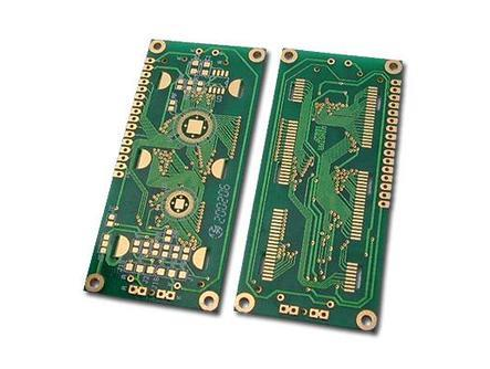
PCB inner and outer layer circuit design rules
Generally, in the entire PCB design, engineers have the most restrictive, finest skills, and the most workload for their wiring design. The layout of printed wires should be short. If it is a high-frequency circuit or dense wiring, the corners of the printed wires should be rounded so that the electrical characteristics of the circuit will not be affected. When double-sided wiring, the wires on both sides should be perpendicular to each other, obliquely crossed or bent to avoid parallel to each other to reduce parasitic coupling.
Secondly, the distance between the wiring and the wire should also be uniform. The excess of the connection between the wire and the pad should be smooth, and there should be no abnormalities such as small sharp corners. If the center distance between the pads is less than the outer diameter of a pad, solder The width of the connecting wire between the pads can be the same as the diameter of the pad; when the center distance between the pads on the PCB is greater than the outer diameter of the pad, the width of the wire should be reduced; when there are three or more on a wire The distance between them should be greater than the width of the two diameters.

The quality of the PCB design will also have a certain impact on its anti-interference ability. In the PCB design, the basic principles of the design must be followed, and the requirements of the anti-interference design should be met to make the circuit obtain the best performance. The printed wires used as the input and output of the circuit should be avoided as far as possible to avoid parallelism, so as not to cause backflow, and add a grounding wire between these wires. The common ground wire of the printed wire should be placed on the edge of the PCB as much as possible, and as much copper foil as the ground wire should be reserved on the PCB, so that the shielding effect is better than a long ground wire, and the transmission line characteristics and shielding effect It is better, and it also plays a role in reducing distributed capacitance.
Special attention should be paid to the fact that some cross circuits must be made in the PCB board and what should be done if it is not allowed? At this time, it can only be solved by "drilling" and "winding", that is, let a lead drill through the gap under the pins of other resistors, capacitors, and transistors, or go around one end of a lead that may cross. . iPCB is a high-tech manufacturing enterprise focusing on the development and production of high-precision PCBs. iPCB is happy to be your business partner. Our business goal is to become the most professional prototyping PCB manufacturer in the world. Mainly focus on microwave high frequency PCB, high frequency mixed pressure, ultra-high multi-layer IC testing, from 1+ to 6+ HDI, Anylayer HDI, IC Substrate, IC test board, rigid flexible PCB, ordinary multi-layer FR4 PCB, etc. Products are widely used in industry 4.0, communications, industrial control, digital, power, computers, automobiles, medical, aerospace, instrumentation, Internet of Things and other fields.