1. PCB board design steps
Generally speaking, the most basic process of designing a circuit board can be divided into three steps.
(1). Design of circuit schematic: The design of circuit schematic is mainly based on PROTEL099's schematic design system (Advanced Schematic) to draw a circuit schematic. In this process, we must make full use of the various schematic drawing tools and various editing functions provided by PROTEL99 to achieve our goal, that is, to obtain a correct and exquisite circuit schematic.
(2). Generate netlist: netlist is a bridge between circuit schematic design (SCH) and printed circuit board design (PCB). It is the soul of PCB board automation. The netlist can be obtained from the schematic circuit diagram or extracted from the printed circuit board.
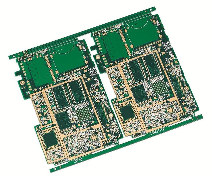
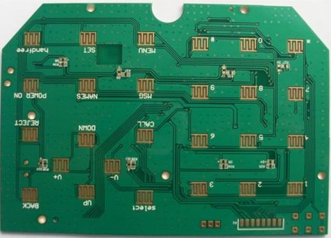
(3). The design of the printed circuit board: The design of the printed circuit board is mainly for another important part of the PCB of PROTEL99. In this process, we use the powerful functions provided by PROTEL99 to realize the layout design of the PCB board, To complete difficult and other tasks.

2. Draw a simple circuit diagram
2.1 Schematic diagram design process Schematic diagram design can be completed according to the following process.
(1) Design the drawing size
After Protel 99/Schematic, we must first conceive the part drawing and design the drawing size. The size of the drawing is determined according to the scale and complexity of the circuit diagram. Setting a suitable drawing size is the first step to design a good schematic diagram.
(2) Set Protel 99/Schematic design environment
Set Protel 99/Schematic design environment, including setting grid size and type, cursor type, etc. Most parameters can also use system default values.
(3) Rotating parts
According to the needs of the circuit diagram, the user removes the parts from the parts library and places them on the drawings, and defines and sets the serial numbers and parts packaging of the placed parts.
(4) Wiring with schematic diagram
Use various tools provided by Protel 99/Schematic to connect the components on the drawing with wires and symbols with electrical meaning to form a complete schematic diagram.
(5) Adjusting the circuit
will make further adjustments and modifications to the preliminarily drawn circuit diagram to make the schematic diagram more beautiful.
(6) Report output
Various reports are generated through various report tools provided by Protel 99/Schematic. The most important report is the network table. The network table is used to prepare for the subsequent circuit board design.
(7) File save and print output” The final step is file save and print output.
The design principles of the single-chip microcomputer control board need to follow the following principles:
(1) In terms of the layout of components, the components related to each other should be placed as close as possible. For example, the clock generator, crystal oscillator, and the clock input of the CPU are all prone to noise, so they should be placed closer. . For those devices that are prone to noise, low-current circuits, high-current circuit switching circuits, etc., keep them away from the logic control circuit and storage circuit (ROM, RAM) of the single-chip microcomputer as much as possible. If possible, these circuits can be made into circuits. Board, this is conducive to anti-interference and improve the reliability of circuit work.
(2) Try to install decoupling capacitors next to key components such as ROM, RAM and other chips. In fact, printed circuit board traces, pin connections and wiring, etc. may contain large inductance effects. Large inductance may cause severe switching noise spikes on the Vcc trace. The only way to prevent switching noise spikes on Vcc traces is to place a 0.1uF electronic decoupling capacitor between VCC and power ground. If surface mount components are used on the PCB board, chip capacitors can be used to directly tighten the components and fix them on the Vcc pin. It is best to use ceramic capacitors, because this type of capacitor has lower electrostatic loss (ESL) and high-frequency impedance, and the temperature and time of the dielectric stability of this type of capacitor are also very good. Try not to use tantalum capacitors, because their impedance is higher at high frequencies. Pay attention to the following points when placing decoupling capacitors:
Connect a 100uF electrolytic capacitor across the power input end of the printed circuit board. If the volume permits, a larger capacity is better. In principle, a 0.01uF ceramic capacitor needs to be placed next to each integrated circuit chip. If the gap of the circuit board is too small to fit, you can place a 1-10 tantalum capacitor for every 10 chips. For components with weak anti-interference ability and large current changes when turned off, and storage components such as RAM and ROM, a decoupling capacitor should be connected between the power line (Vcc) and the ground line. The lead of the capacitor should not be too long, especially the high-frequency bypass capacitor cannot have lead.
(3) In the single-chip microcomputer control system, there are many types of ground wires, such as system ground, shield ground, logic ground, analog ground, etc. The reasonable layout of the ground wire will determine the anti-interference ability of the PCB board. When designing ground wires and grounding points, the following issues should be considered:
The logic ground and the analog ground should be wired separately and cannot be used together. Connect their respective ground wires to the corresponding power ground wires. When designing, the analog ground wire should be as thick as possible, and the grounding area of the terminal should be enlarged as much as possible. Generally speaking, it is best to isolate the input and output analog signals from the microcontroller circuit through optocouplers. When designing the printed circuit board of the logic circuit, the ground wire should form a closed loop form to improve the anti-interference ability of the circuit. The ground wire should be as thick as possible. If the ground wire is very thin, the resistance of the ground wire will be large, causing the ground potential to change with the current change, causing the signal level to be unstable, resulting in a decrease in the anti-interference ability of the circuit. When the wiring space allows, ensure that the width of the main ground wire is at least 2 to 3 mm, and the ground wire on the component pin should be about 1.5 mm.