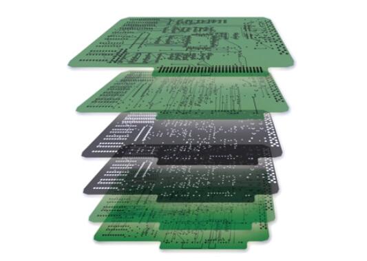
Summary of Multilayer Board Design Principles
(1) The components used on the printed circuit board should be correct, including the size, spacing, brush number, frame size and direction indication of the brush.
(2) The positive and negative values of polar parts (electrolytic capacitors, diodes, transistors, etc.) should be described in the parts library and printed circuit.
(3) The PIN number of the PCB part must be the same as the part shown in the figure. For example, the previous chapter introduced the inconsistency between the DOODES printed circuit library components and the piercing numbers in the book library.
(4) The size of the radiator must be considered in the packaging of the components that require a radiator. The part and the heat sink can be collected together.
(5) The inner diameter of the part and the slice of the part must match. The inner diameter of the skate should be slightly higher than the size of the component for installation.
2. Disposal requirements of printed circuit components
(1) The components of the same functional module must be as close as possible.
(2) The same type of power supply and ground network components are arranged together as much as possible, so that the electrical connection between them can be completed through the internal layer.
(3) The interface components must coexist next to each other, and the interface type must be provided by a chain. The connection direction should usually be far away from the circuit board.
(4) Power conversion components (transformers, DC/DC converters, three-terminal regulators, etc.) should have enough space for heat dissipation.
(5) The slicing or reference point of the component must be placed on the gate point that is conducive to wiring and aesthetics. The filter capacitor can be placed on the bottom of the chip, close to the power supply and ground of the chip.

(7) The first part or the first direction mark must be marked on the printed circuit, and cannot be reassembled by parts.
(8) The component label must be close to the component, uniform size, clear direction, and not overlap with skates and passages, or be placed in the component coverage area after installation.
3. Wiring requirements for the card
(1) Power supplies of different voltage levels must be separated, and power cables should not be handed over.
(2) The route uses a 45-degree angle or an arc angle, and no tip angle is allowed.
(3) The wiring of the printed circuit board is directly connected to the center of the chip. The width of the yarn connected to the skate should not exceed the outer diameter of the skate.
(4) The line width of the high-frequency signal line shall not be less than 20 minutes. It surrounds the outside wire and isolates other ground wires.
(5) There is no wiring under the interference source (DC/CC converter, crystal oscillator, transformer, etc.) to avoid interference.
(6) Increase the cables for food and land as much as possible. When space permits, the width of the power cord is not less than 50 meters.
(7) The line width of low-voltage and low-current signals is 9 to 30 meters, which is as thick as possible when space permits.
(8) The spacing between signal wires should exceed 10 meters, and the spacing between wires exceeding 20 meters should be spaced.
(9) The circuit width of the current signal should be greater than 40 meters, and the interval should be greater than 30 meters.
(10) The minimum size of the hole is 40 meters in outer diameter and 28 meters in inner diameter. When yarns are used to connect the upper layer and the lower layer, solder pads are more preferable. No signal line can be set on the inner layer.
(11) The width of the interval between the inner layers is not less than 40 meters. Copy this website code to your website to set up a ballot box on your website. To deposit copper on the upper and lower layers, it is recommended that the line width be greater than the gate width to completely cover the free space without leaving any dead copper. At the same time, the spacing should be greater than 0.762mm (30mm) (30mm) and other lines (you can determine a safe spacing before copper installation, and change the initial spacing after copper laying).
(12) After wiring, apply a drop of water to the skating.
(13) The outside of peripheral equipment and metal modules.
4.2. Conditions for polychlorinated biphenyl superposition
(1) The food plan should be close to the ground level, closely connected on the ground, and set up on the ground.
(2) The signal layer should be adjacent to the inner layer, not directly adjacent to other signal layers.
(3) Separate digital circuits from analog circuits. If conditions permit, set up analog and digital signal line layers and take protective measures. If the same signal layer is required, isolation bands and quality lines are needed to reduce interference; the power and quality of the analog and digital circuits must be separated and not mixed.
(4) The high-frequency circuit has high external interference. It is best to organize it separately, and use the dielectric signal layer with the inner layer directly adjacent to the upper and lower layers to reduce external interference. Use a copper film containing: no layer .
This chapter mainly introduces the design phase of multilayer printed circuit boards, including the selection of the number of multilayer cards and the choice of stacking structure; the same and different multilayer boards and double-layer boards; creating and trusting a single middle layer and inner layer in a multilayer board the design of.
According to the steps listed in this chapter, the player successfully completed the preliminary design of the multilayer printed circuit.
ipcb is a high-precision, high-quality PCB manufacturer, such as: isola 370hr PCB, high-frequency PCB, high-speed PCB, ic substrate, ic test board, impedance PCB, HDI PCB, Rigid-Flex PCB, buried blind PCB, advanced PCB, microwave PCB, telfon PCB and other ipcb are good at PCB manufacturing.