PCB design process of 6 layer PCB circuit board
SMT chip processing manufacturers introduce in detail the PCB design process of the circuit board and the issues that should be paid attention. In the design process, different layout principles are adopted for common components and some special components; compare the advantages and disadvantages of manual wiring, automatic wiring and interactive wiring; introduce PCB circuits and the methods adopted to reduce interference between circuits Related measures. Combining personal design experience, take the PCB design of ARM-based, autonomous mobile embedded system core board as an example, briefly introduce the PCB design process of the four-layer circuit board and related issues that should be paid attention to.
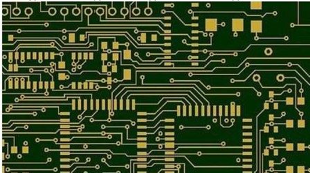
Printed circuit boards (PCBs) play a role in supporting circuit elements and devices in electronic products, and at the same time provide electrical connections between circuit elements and devices. In fact, the design of PCB is not only about arranging and fixing the components, but also the pins connecting the components are so simple. Its quality has a great influence on the anti-interference ability of the product. It even plays a decisive role in the performance of future products. With the rapid development of electronic technology, the dimensions of components and products have become smaller and smaller, and the working frequency has become higher and higher, which greatly increases the density of components on the PCB, which also increases the difficulty of PCB design and processing. . Therefore, it can be said that PCB design is always one of the most important contents in the development and design of electronic products. 1 Layout The so-called layout is to rationally arrange all the components in the circuit diagram on a PCB with a limited area. From the signal point of view, there are mainly three types of digital signal circuit boards, analog signal circuit boards and mixed signal circuit boards. When designing a mixed-signal circuit board, we must carefully consider and place the components on the circuit board by hand to separate the digital and analog components.

In the process of arranging the PCB layout, the most critical issue is: switches, buttons, knobs and other operating parts and structural parts (referred to as "special components"), etc., must be arranged in advance at designated (appropriate) positions. After placement, you can set the properties of the components and select the LOCK item, so that you can avoid moving them by mistake in the future; and for the location of other components, you must take into account the wiring layout rate and the best electrical performance. Optimization, and many factors such as future production technology and cost. The so-called "balance" is often a challenge to the level and experience of the design staff.
The layout principle of special components
1. The wiring between components should be shortened as much as possible, and try to reduce their distribution parameters and mutual electromagnetic interference. Those components that are susceptible to electromagnetic interference should not be placed too close together, and the input and output components should be as far away as possible from each other.
2. There may be a high potential difference between some components or wires, so the distance between them should be increased to avoid accidental short circuits caused by discharge; at the same time, from a safety point of view, components with high voltage should be as far as possible Arrange in a place that is not easy to reach during debugging.
3. For large devices with a mass of more than 15g, they should be fixed with brackets before welding. Those large, heavy, and heat-generating components should not be mounted on the printed circuit board, but should be mounted on the chassis bottom plate of the whole machine; and the heat dissipation problem should be considered. Except for temperature-protected devices).
4. For the layout of adjustable components such as adjustable potentiometers, inductors, variable capacitors, and micro switches, the structural requirements of the whole machine should be considered. If it is adjusted inside the machine, it should be placed on the printed circuit board where it is convenient for adjustment; if it is adjusted outside the machine, its position should be adapted to the position of the adjustment knob on the chassis panel.
The layout of common components
1. Arrange the position of each circuit unit according to the circuit flow, so that the layout is convenient for signal circulation, and try to keep the signal in the same direction.
2. Take the core component of each functional circuit as the center and lay out around it. The components should be evenly, neatly and compactly arranged on the PCB. Minimize and shorten the leads and connections between devices.
3. For circuits operating at high frequencies, the distributed parameters between components must be considered. Under normal circumstances, the circuit should be arranged in parallel as much as possible, not only can achieve the beautiful effect, but also easy to install welding and mass production.
4. The components located at the edge of the circuit board are generally not less than 2mm away from the edge of the circuit board; the best shape of the circuit board is rectangular, and its aspect ratio can be 3:2 or 4:3. When the size of the circuit board is larger than 200mm*150mm, the mechanical strength of the circuit board should be considered. If in the actual design process, the required size of the PCB board cannot be determined at the beginning, the design can be slightly larger. After the PCB design work is completed, you can select Design-Board Shape-Redefine Board Shape in Protel DXP to properly cut the original PCB.
In addition, according to my actual work experience, if you want to expand or reduce some functions of the existing circuit board, you need to redesign a new PCB. In the actual layout, you can refer to the layout on the motherboard and manually The components are arranged in appropriate positions; during the wiring process, adjustments are made according to actual needs to further improve the distribution rate.
2 Wiring Wiring is to connect all the wires according to the schematic diagram by setting the wiring diagram of the copper foil after the layout. Obviously, the reasonable degree of the layout will directly affect the success rate of the wiring, so it is often necessary to make appropriate adjustments to the layout during the entire process of wiring. Wiring design can use double-layer wiring and single-layer wiring; for extremely complex designs, multi-layer wiring schemes can also be considered.
In PCB design, wiring is an important step to complete product design. It can be said that all the previous preparations are done for it. PCB wiring includes single-sided wiring, double-sided wiring and multilayer wiring. There are two ways of routing: automatic routing and interactive routing.
In PCB design, designers often want to be able to use automatic routing. Under normal circumstances, it is no problem to use automatic wiring for pure digital signal circuit boards (especially low signal level and low circuit board density). However, in the design of analog signals. When mixed-signal or high-speed circuit boards are used, if automatic wiring is also used, problems may occur, and may even cause serious circuit performance problems.
At present, although there are already some automatic wiring tools that are very powerful, they can usually reach 100% of the distribution rate, but the overall appearance is not very beautiful, sometimes the wiring arrangement is disorderly, and the wiring between the two pins is not the shortest (Optimal) path. For designs with relatively complicated circuits, please try not to use automatic wiring completely. It is recommended that before adopting automatic routing, first use an interactive method to pre-wire those lines with strict requirements. At the same time, the edges of the input end and the output end should be avoided adjacent to parallel to avoid reflection interference; the wiring of two adjacent layers should be perpendicular to each other, and parallelism is prone to parasitic coupling. This constraint can be added in the wiring rules. The distribution rate of automatic routing depends on a good layout. Wiring rules should be set in advance, including the number of bends, the number of vias, and the number of steps. Generally, explore the city line first, quickly connect the short line first; then perform the labyrinth wiring, first optimize the global wiring path of the line to be laid, it can disconnect the laid line according to the need, and re-route it, To improve the overall effect. During manual wiring, in order to ensure the correct implementation of the circuit, some general design rules need to be followed: try to use the ground plane as the current loop; separate the analog ground plane from the digital ground plane; if the ground plane is separated by the signal line, then to reduce the ground For the interference of the current loop, the signal trace should be perpendicular to the ground plane; the analog circuit should be placed as close as possible to the edge of the circuit board, and the digital circuit should be placed as close as possible to the power connection end. This is done to reduce the di/dt effect caused by the digital switch.
PCB circuit and circuit anti-jamming measures Anti-jamming design has a close relationship with the specific circuit, and it is also a very complicated technical problem. Here are some brief introductions based on the experience in the PCB design process. 1. The design of the power cord. According to the size of the PCB current, make the width of the power line as thick as possible (in the wiring design rules, you can make new constraint rules for the line width of the power line and the ground line separately), reduce the loop resistance, and pay special attention to the power line, The power supply direction of the ground wire is opposite to the transmission direction of data and signals, which helps to enhance the anti-noise ability. 2. The design of the ground wire. The ground wire is both a special power wire and a signal wire. In addition to following the design principles of the power cord, it should also be achieved: digital ground and analog ground should be separated; if there are both logic circuits and linear circuits on the circuit board, they should be separated as much as possible; low-frequency circuit grounds should be as single as possible. Points are connected in parallel, and if there are difficulties in actual wiring, they can be partially connected in series and then connected in parallel; high-frequency circuits should be connected in series with multiple points. The ground wire should be short and thick. Use grid-like copper around the high-frequency components as much as possible; Try to widen the width of the power and ground wires. It is best to make the ground wires wider than the power wires. The relationship between their widths is ground wire>power wire>signal wire. 3. The grounding of the digital circuit system forms a closed loop, that is, forms a ground network, which can improve the anti-noise ability. 4. Digital current should not flow through analog devices, and high-speed current should not flow through low-speed devices. 5. Add decoupling capacitors between the power ground wires to improve the anti-interference ability of the power circuit.