What is impedance?
In electricity, the resistance to the current in printed circuit board is often called impedance. The unit of impedance is ohm, usually expressed as Z, and is a complex number:
Z = R (omega I L - 1 / (C) omega)
Specifically, impedance can be divided into two parts, resistance (real part) and reactance (imaginary part).
The reactance includes capacitive reactance and inductive reactance. The current obstruction caused by capacitance is called capacitive reactance, and the current obstruction caused by inductance is called inductive reactance.
Ideal model for impedance matching
Most RF engineers have encountered the problem of matching impedances. in layman's terms, impedance matching is designed to ensure efficient transmission of signals or energy from the "source" to the "load".
The ZZ ideal model, of course, expects the output impedance of the Source terminal to be 50 ohms, the impedance of the transmission line to be 50 ohms, and the input impedance of the Load terminal to be 50 ohms all the way down, which is Z ideal.

However, the actual situation is that the source impedance will not be 50ohm, and the load impedance will not be 50ohm, which requires several impedance matching circuits.
And the matching circuit is composed of inductance and capacitance, at this time we need to use capacitance and inductance for impedance matching circuit debugging, in order to achieve optimal RF performance.
Impedance matching method
There are two main methods of impedance matching, one is to change the impedance force, the other is to adjust the transmission line.
To change the impedance force is to adjust the load impedance value through the series and parallel connection of capacitance, inductance and load to match the source and load impedance.
Adjust the transmission line is to lengthen the distance between the source and the load, with capacitance and inductance to adjust the impedance force to zero.
At this point, the signal will not be emitted and the energy can be absorbed by the load.
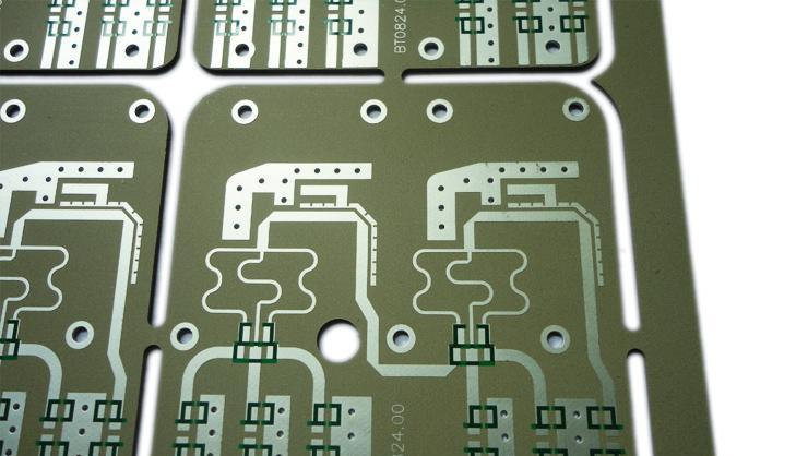
In high-speed PCB wiring, the wiring impedance of digital signal is generally designed as 50 ohm. It is generally stipulated that the coaxial cable base band is 50 ohms, the frequency band is 75 ohms, and the twisted pair (difference) is 85-100 ohms.
Example for impedance matching: Ringing
I once encountered the problem of ringing when measuring electrical signals in a project.
Because any transmission line inevitably has lead resistance, lead inductance and stray capacitance, a standard pulse signal after passing through a long transmission line is prone to upsurge and ringing phenomenon. A large number of experiments show that lead resistance can reduce the average amplitude of pulse. The existence of stray capacitance and lead inductance is the root cause of upshot and ringing. Under the condition of the same rising time of pulse front, the higher the lead inductance is, the more serious the upsurge and ringing phenomenon will be. The larger the stray capacitance is, the longer the rise time of waveform is. As the lead resistance increases, the pulse amplitude decreases.
If a change in impedance is felt during signal transmission, signal reflection occurs. This signal may be a signal from the driver or a reflected signal from the remote end. According to the formula of reflection coefficient, when the signal feels a smaller impedance, negative reflection will occur, and the reflected negative voltage will cause the signal to produce a downdraft. The signal is reflected multiple times between the driver and the remote load, resulting in a ringing signal. The output impedance of most chips is very low, and if the output impedance is less than the characteristic impedance of the PCB wiring, the signal will inevitably ring in the absence of source end to end connection.
In actual circuits, the following methods are used to reduce and suppress upstroke and ringing.
(1) series resistance. The amplitude of the pulse can be reduced by using a transmission line with a large resistance or by artificially connecting a proper damping resistance, so as to reduce the upsurge and ringing degree. However, when the value of the incoming resistance is too large, not only the pulse amplitude decreases too much, but also the front edge of the pulse is delayed. Therefore, the damping resistance value in series should be appropriate, and non-inductive resistance should be selected, and the connection position of resistance should be close to the receiving end.
(2) Reduce lead inductance. Try to reduce the lead inductance of the line and transmission line is the basic method, the general principle is:
Try to shorten the lead length
Width of thick wire and printed copper foil
Reduce the transmission distance of the signal
These problems should be paid more attention to when the components with small inductance are used, especially when the pulse signal with very steep front is transmitted
(3) As the equivalent inductance and capacitance of the load circuit can also affect the sending end, so that the pulse waveform produces upsurge and ringing, therefore, the equivalent inductance and capacitance of the load circuit should be minimized. Especially when the grounding wire of the load circuit is too long, the inductance and stray capacitance of the grounding wire are considerable, and their influence cannot be ignored.
(4) The signal line in the logical digital circuit can increase the pull-up resistance and ac terminal load, as shown in Figure 6. A pull-up resistor is available to pull the logical high level of the signal up to 5V.The access of ac terminal load circuit does not affect the driving ability of tributaries, nor does it increase the load of signal line, while the high-frequency ringing phenomenon can be effectively suppressed.
The above ringing is not only related to the circuit condition, but also closely related to the rise time of the pulse front. Even if the circuit conditions are the same, when the rise time of the pulse front is very short, the peak of the upsurge will be greatly increased. Generally, the possibility of upsurge and ringing is considered for the pulse with the rise time of the leading edge less than 1. Therefore, in the selection of pulse signal frequency, it should be considered that on the premise of meeting the speed requirements of the system, the signal that can choose the lower frequency should not choose the high frequency signal; If not necessary, it should not be excessively required that the leading edge of the pulse be very steep. This fundamentally eliminates the impact and ringing audio-visual benefits.
Application of Smith circle diagram in RF Matching circuit debugging
The following information can be reflected in the Smith circle diagram: impedance parameter Z, admittance parameter Y, quality factor Q, reflection coefficient, standing wave coefficient, noise coefficient, gain, stability factor, power, efficiency, frequency information and other resistance parameters.
Is not a face meng, we still look at the impedance circle diagram:
The principle of impedance circle diagram is to use the one-to-one correspondence between input impedance and voltage reflection coefficient to express normalized input impedance in the polar coordinate system of reflection coefficient, and its characteristics are summarized as follows:
The impedance of upper semicircle is inductive reactance and that of lower semicircle is capacitive reactance
The real axis is pure resistance and the unit circle is pure reactance
The right half axis of the real axis are all voltage wave belly points (except open circuit points), and the left half axis are voltage wave nodes (except short circuit points).
Matching point (1,0), open circuit point (∞, ∞) and short circuit point (0,0)
Two special circles: the one with the greatest Z is the pure reactance circle, and the one tangent to the virtual axis is the matching circle
There are two directions of rotation: counterclockwise to the load and clockwise to the wave source
The admittance circle graph and impedance circle graph are mutually centrosymmetric. The same circle graph can be used as impedance circle graph or admittance circle graph, but it cannot be used as admittance circle graph if it is used as impedance circle graph during each YC operation.
Smith's circle shows some interesting features:
A variable inductor/capacitor is connected in series or parallel before the load, as shown in the four diagrams on the left side of the figure below, resulting in several curves on the right side of the Smith circle.
Corresponding to Smith impedance circle and admittance circle, their motion trajectory is as follows:
With a Smith impedance circle, the series inductor turns clockwise and the series capacitor turns counterclockwise
When using Smith admittance circles, the shunt inductor rotates counterclockwise and the shunt capacitance rotates clockwise