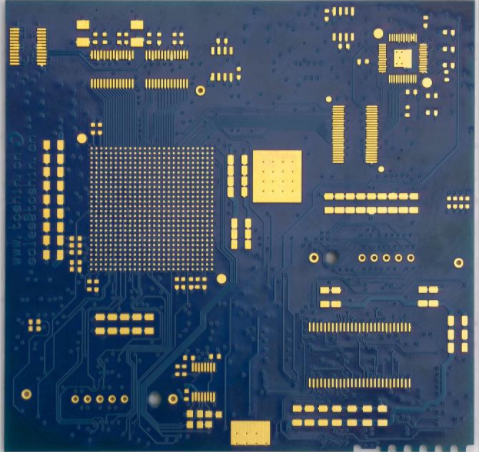
1. Reasonable assembly layout of PCB components is the basic prerequisite for designing high-quality PCB drawings.
The component layout requirements mainly include installation, stress, heating, signal, and aesthetics.
1.1. Installation refers to the specific application. In order to successfully install the circuit board into the chassis, shell, and slot, there will be no space interference, short-circuit and other accidents, and a series of basic requirements have been put forward for the designated connector in the designated position on the chassis or shell.
1.2. Mandatory circuit boards should be able to withstand various external forces and vibrations during installation and operation. For this reason, the circuit board should have a reasonable shape, and the positions of various orifice plates (screw holes, special-shaped holes) should be arranged reasonably. Generally, the distance between the hole and the edge of the board is at least greater than the diameter of the hole. At the same time, it should also be noted that the weakest part of the board caused by the special-shaped hole should also have sufficient bending strength.

The device shell of the connector directly "stretched" on the board must be reasonably fixed to ensure long-term reliability.
1.3. Heating For high-power, serious heating devices, in addition to ensuring heat dissipation conditions, they must also be placed in a suitable location. Especially in complex analog systems, special attention should be paid to the adverse effects of the temperature field generated by these devices on the fragile preamplifier circuit.
Generally, the part with high power should be made into a separate module, and certain heat insulation measures should be taken between the signal processing circuits.
1.4. Signal signal interference is the most important factor to be considered in PCB layout design. Some of the most basic aspects are: separation or even isolation of weak signal circuits and strong signal circuits; separation of AC part from DC part; separation of high frequency part from low frequency part; pay attention to the direction of signal line; layout of ground line; proper shielding, filtering, etc. measure.
1.5. Beauty should not only consider the neat and orderly placement of components, but also the beautiful and smooth lines. Because the general layman sometimes emphasizes the former more, in order to one-sidedly evaluate the advantages and disadvantages of the circuit design, for the image of the product, when the performance requirements are not demanding, the predecessor should be given priority. However, in high-performance applications, if you must use a double-sided board, and the circuit board is also encapsulated in it, it is usually invisible, and you should give priority to the aesthetics of the lines.
2. Wiring principle The following is a detailed description of some anti-jamming measures that are not common in the literature.
Taking into account the actual application, especially in the trial production of products, there are still a large number of double panels, the following content is mainly used for double panels.
2.1. PCB wiring "aesthetics"
Avoid right angles when turning, and try to use diagonal or arc transitions. The walking line should be neat and orderly, divided into centralized arrangement, not only can avoid the mutual interference of signals of different nature, but also easy to check and modify.
For digital systems, there is no need to worry about interference between signal lines in the same camp (such as data lines, address lines), but control signals such as read, write, and clock should be isolated and preferably protected by ground.
For large-area paving (discussed further below), the ground wire (actually should be the ground "surface") and the signal wire should be kept at a reasonable equal distance as much as possible, and they should be as close as possible under the premise of preventing short circuit and leakage.
For weak current systems, the ground wire should be as close as possible to the power wire.
For systems using surface sticker components, the signal line should be as full as possible in the positive direction.
2.2. There are many explanations on the importance and layout principle of the grounding wire in the grounding layout literature, but there is still a lack of detailed and accurate introduction to the grounding wire layout in the actual PCB. My experience is that in order to improve the reliability of the system (not just to make experimental prototypes), the ground wire cannot be overemphasized, especially in weak signal processing.