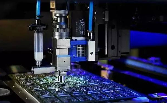
The following is an introduction to the PCB circuit board design of the 3.3V dual 14-bit ADC:
1. Introduction to MAX12557
The MAX12557 is a dual, 3.3V, 14-bit analog-to-digital converter (ADC) with a fully differential broadband sample/hold (T/H) input to drive an internal quantizer. The MAX12557 is optimized for low power consumption, small size, and high dynamic performance, and is suitable for intermediate frequency (IF) and baseband sampling applications.
The general recommendations for the circuit design of the MAX12557 are as follows.
(1) Pins 2 and 3, INAP and INAN: In order to obtain the best AC performance, according to the specific application, a certain capacitance should be connected in parallel between these pins and the ground, and the capacitance range is 5.6-12pF. These capacitors may be included in the anti-aliasing filter driving the ADC and should be placed on the top layer of the PCB.

(2) Pin 6, COMA: COMA is bypassed to GND through a 2.2μF ceramic capacitor with good high frequency performance.
(3) Pin 7, REFAP: Bypass REFAP to GND through a high-frequency ceramic capacitor (maximum 1.0μF) located on the top of the PCB. All REFAP connections should be as short as possible.
(4) Pin 8, REFAN: Bypass REFAN to GND through a high-frequency ceramic capacitor (maximum 1.0μF) located on the top layer of the PCB. All REFAN connections should be as short as possible. (5) Pin 10, REFBN: Bypass REFBN to GND through a high-frequency ceramic capacitor (maximum 1.0μF) located on the top layer of the PCB. All REFBN connections should be as short as possible.
(6) Pin 11, REFBP: Bypass REFBP to GND through a high-frequency ceramic capacitor (maximum 1.0μF) located on the top layer of the PCB. All REFBP connections should be as short as possible.
(7) Pin 12, COMB: COMB is bypassed to GND through a 2.2μF ceramic capacitor with good high frequency performance.
(8) Pin 15 and Pin 16, INBN and INBP: In order to obtain the best overall AC performance, according to the specific application, a certain capacitance should be connected in parallel between these pins and the ground, the capacitance value is 5.6-12pF. These capacitors may be included in the anti-aliasing filter driving the ADC and should be placed on the top layer of the circuit board.
(9) Pins 23~26, 61~63 (VDD): Use a 1.0μF ceramic capacitor with good high frequency performance and a ceramic capacitor with good high frequency performance of 2.2μF or more in parallel to bypass VDD to GND.
(10) Pins 27, 43, 60 (OVDD): Use a 1.0μF ceramic capacitor with good high frequency performance and a ceramic capacitor with good high frequency performance of 2.2μF or more in parallel to bypass VDD to GND.
(11) Pins 28 to 41 (D0B to D13B): Add series resistance to the data output pins. This series resistor can limit the high-frequency edge current flowing from the output driver and returning to the internal GND of the chip. Choose an appropriate resistance value so that the RC time constant formed by the combination of it and the load capacitance is about 1 ns. You can use a very small and very cheap resistor bank, such as PCB company's EXB-2HV-221J.
(12) Pins 45 to 58 (D0A to D13A): Add series resistance on the data output pins. This series resistor can limit the high-frequency edge current flowing from the output driver and returning to the internal GND of the chip. Choose an appropriate resistance value so that the RC time constant formed by the combination of it and the load capacitance is about 1 ns. You can use a very small and very cheap resistor bank, such as PCB company's EXB-2HV-221J.
(13) PCB internal reference voltage output pin (pin 67, REFOUT): The voltage of this REFOUT is 2.048V, which can output 1mA current. When using an internal reference, REFOUT is directly connected to REFIN, or the output voltage of REFOUT is divided by a resistor divider to set the REFIN input voltage. REFOUT is bypassed to GND through a ceramic capacitor with good high-frequency performance and a value greater than or equal to 0.1μF.
(14) Single-ended reference analog input (pin 68, REFIN): For PCB internal reference and external reference buffer operating modes, a 0.7-2.3V reference voltage can be applied to REFIN. Within the specified operating voltage range, REFIN has an input impedance greater than 50MΩ, and the differential reference voltage (VREF_P-VREF_N) is generated by REFIN. In PCB internal reference mode and external reference buffer mode, REFIN is bypassed to GND through a high-frequency ceramic capacitor with good performance and a value greater than or equal to 0.1μF. In the unbuffered external reference mode, connect REFIN to GND.