What is the process of PCBA design?
The PCBA design service is very suitable for small and medium-sized enterprises or individuals without a self-built design team. The PCBA design and processing refers to the industry analysis of the customer’s products and the positioning of the customer’s demand for the product, and the customer’s concept is transformed into concrete and feasible The technical plan is continuously modified and optimized to finally form a PCBA plan. After that, the product is manufactured and the concept is transformed into a physical product, so as to seize the market for the company and achieve profitability. So what is the process of PCBA design and processing?
The first is to communicate with the professional design team, and clearly express the product's ideas, functional requirements, and appearance requirements. The designer will give the PCBA design and processing according to the customer's needs. After confirming the PCBA design and processing, select the materials for the product, and select the various components required by the product, such as capacitors, batteries, CPU, IC, etc., which determine the endurance of the product.

Then generate the proofing file, and the engineer analyzes the PCB proofing file in a targeted manner, further optimizes the product, improves the quality of the product, and reduces the defective and after-sales service costs. Product proofing is carried out, product quality is strictly controlled, and all links are controlled. After the product is no problem, mass production can be quickly realized, and the customer's demand for pushing the product into the market can be quickly realized. This is the PCBA design process.
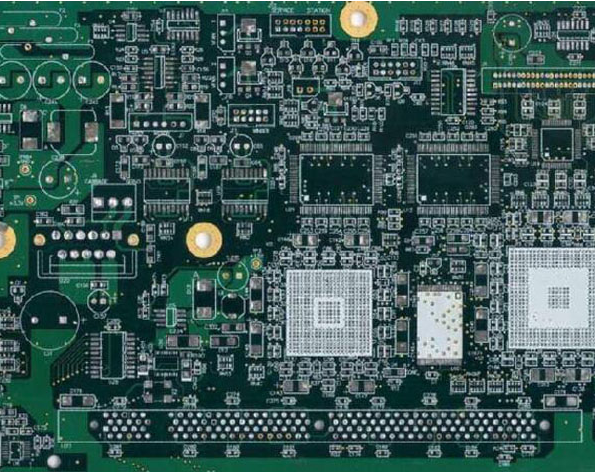
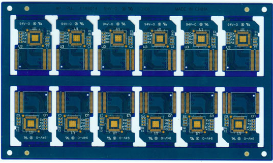
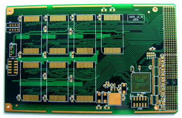
Manual PCB board production process
As we all know, PCB board is an important part of modern electronics, and it is also indispensable, but most people know very little about its production process, so let's take a look together.
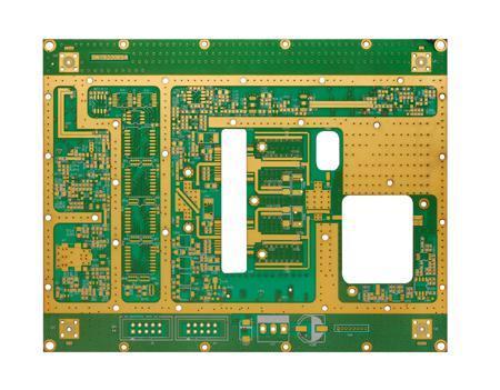
The PCB manufacturing process begins with a PCB "substrate" made of glass epoxy (Glass Epoxy) or similar materials. The first step of the production is to draw the wiring between the parts by light. The method is to use the negative transfer (Subtractive transfer) method to "print" the circuit negative of the designed PCB circuit board on the metal conductor.
Next, the drilling and electroplating required to connect the components can be performed on the PCB board. After drilling by machines and equipment according to drilling requirements, the inside of the hole must be electroplated (Plated-Through-Hole technology, PTH). After the inside of Kongbi is metal treated, the inner layers of the circuit can be connected to each other.
Before starting electroplating, be sure to clean out the debris in the hole. This is because the resin epoxy will produce some chemical changes after heating, and it will cover the internal PCB layer, so it must be removed first. Both cleaning and electroplating actions are completed in the chemical process. Next, the solder mask (solder mask ink) needs to be covered on the outermost wiring, so that the wiring will not touch the electroplated part.
Then, the various components are printed on the circuit board to mark the position of the parts. It cannot cover any wiring or gold fingers, otherwise it may reduce the solderability or the stability of the current connection. In addition, if there is a metal connection part, the "golden finger" part is usually plated with gold at this time, so that high-quality current connection can be ensured when the expansion slot is inserted.
The last step is testing. To test whether the PCB has a short circuit or open circuit, you can use optical or electronic testing. The optical method uses scanning to find defects in each layer, and the electronic test usually uses a flying-probe to check all connections. Electronic testing is more accurate in finding short circuits or open circuits, but optical testing can more easily detect incorrect gaps between conductors.