1.PCB handles the problems of power bus design
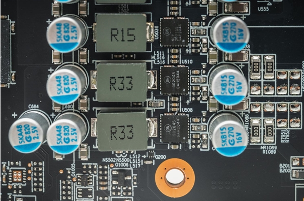
There is an appropriate capacitor near the power supply pin of the IC, and the ic output voltage can jump quickly. However, the problem will not stop here. Since the capacitor is a characteristic of finite frequency response, the capacitor cannot generate the harmonic power required to cleanly drive the output of the full-band IC. In addition, the resulting transient voltage on the power bus forms a voltage drop across the decoupling path, which is the main cause of common-mode EMI interference. How should these problems be solved?
Compared with the circuit board on the IC, the power layer of the peripheral IC is regarded as an excellent high-frequency capacitor for recovering some of the energy leaked from the discrete capacitors to the high-frequency energy provided by the clean output. Moreover, because the excellent power layer inductance is small and the inductance of the synthesized transient signal is also small, the common mode EMI is reduced.
Of course, the wiring of the power layer to the IC power pin is a faster rise of the digital signal, because it is better to connect directly to the pad IC power pin layout, it is necessary to describe separately, as short as possible you must.

In order to control common-mode EMI, it is a decoupling power layer that must have a sufficiently low inductance to be useful, and it must be appropriately designed as a power layer and paired. Someone may ask, how good is it? The answer to the question depends on the hierarchical structure of the power supply, the materials between the layers and the operating frequency (a function of IC rise time). Generally, the power layer spacing is 6 mils, the interlayer is FR4 material, and the equivalent capacitance per square inch of power level is about 75 pF. Obviously, the smaller layer spacing is the larger capacitance.
The 300PS 100 rise time of this device is not much. According to the current development speed of IC, the rise time in the range of 100~300PS occupies a high proportion. Circuits with a rise time of 100 to 300 ps will not impose a 3 mil interval for most applications. At this time, the interlayer spacing of less than 1 mil is passed, and it is necessary to use a high dielectric constant material to replace the FR4 dielectric material. Now, ceramics and ceramic plastics can meet the design requirements of 100 ps and 300 ps rise time circuits.
New materials and methods, but are subject to future use, are used from the usual single-day interval and FR4 dielectric material 6mil 3 rise time circuit is 3ns, often high-end processing harmonics and making the transient signal low enough is enough, that is Common mode EMI may drop very low. In this article, the PCB stackup design example assumes a layer pitch of 3 to 6 mils.
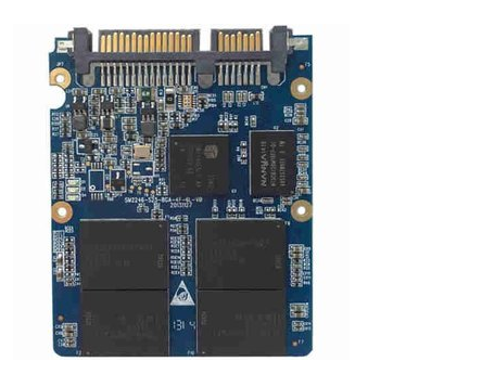
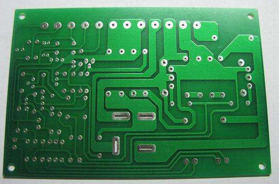
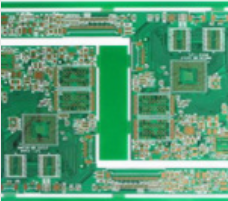
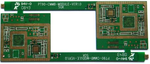
2.Problems with PCB copy board
There are several potential problems with the 4-layer board design. First of all, the thickness of the traditional 62mil layer board can range from the signal layer to the outer layer. Inside, the power layer and the ground layer between the power layer and the ground layer are still too large.
If you consider cost requirements first, please consider the following two traditional 4-layer board options. These two solutions can improve EMI suppression performance, but are only suitable for applications with a sufficiently low on-board component density and sufficient area around the component (where the required power cladding is located).
If the two power layers of the same voltage source require large output current, the circuit board must be woven into two sets of power and ground layers. In this case, an insulating layer is provided between each pair of power and ground layers. This provides us with the same two pairs of impedance power buses as ours. If the power layer stacking causes the impedance to be unequal, the shunt is not uniform, the transient voltage is much larger and the EMI increases sharply.
Remember that each pair of power and ground planes will be created for a different power source, because if the board has multiple different power supply voltages, multiple power planes are required. In either case, when determining the location of the power and ground planes of the circuit board, the manufacturer’s requirements for balanced structures must be kept in mind.
Most engineers are designing 62-mil-thick circuit boards. There are no blind holes or embedded holes on traditional printed circuit boards, so the discussion about the circuit board hierarchy and stacking is limited to this. If the thickness of the circuit board is too large, the proposed layering scheme may not be ideal. In addition, the processing steps of the circuit boards with blind holes and buried holes are different, and the lamination method of this article cannot be applied.
The thickness, through holes and number of layers in the circuit board design are not the key to solving the problem. Ensure the bypass and decoupling of the power bus, minimize the transient voltage of the power layer and the ground layer, and shield the world is the key to high-quality stacking. Ideally, there is an insulating layer between the signal line layer and its return ground layer, and the spacing (or one or more) of the matching layer should be as small as possible. Based on these basic concepts and principles, we can always design a circuit board that meets the design requirements. Because the rise time of IC is already very short, in order to solve the problem of EMI shielding, the technique described in this article is necessary.