In the absence of electronic production materials and only PCB circuit board prototypes, in order to shorten the development time and save development costs, it is a very economical way to use the prototype to copy the board.
Usually circuit board copying and proofing include circuit board cloning, component replacement, making BOM list, exporting schematic diagrams, prototype production and other items; among them, circuit board cloning includes single board cloning, complete circuit board cloning (ie secondary development).
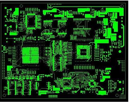
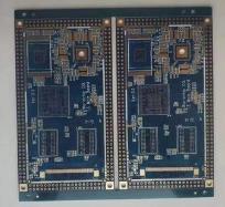
The following is an introduction to the specific process and operation method of the eight-layer PCB copy board:
Step 1: Preparation
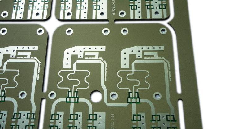
Get a good circuit board to see if there are any components with a high position. If so, first make a detailed record of the component location number, component packaging, temperature value, etc. You must scan it as a backup before disassembling the components. After removing the higher components, SMD and some smaller components are left. At this time, perform a second scan to record the image. It is recommended that the resolution be 600dpi. Be sure to remove the dirt on the PCB surface before scanning to ensure that the IC model and the characters on the PCB are clearly visible on the picture after scanning.

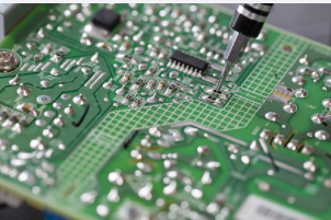
Step 2: Disassemble components and make BOM
Use a small air gun to heat the components to be disassembled by Huai, clamp them with tweezers and let the pipe wind blow them away. Remove the resistor first, then the capacitor, and finally the IC. And record whether there are any components that have been dropped and previously installed reversely. Before disassembling, prepare a form with record items such as tag number, package, model, value, etc., and paste double-sided tape on the column of the component record. After writing down the position number, paste the removed components one by one to the corresponding position of the position number. After disassembling all the components, use the bridge to measure their values (some components will change their values under the action of high temperature, so they should be After all the devices have cooled down, perform the measurement again, and the measured values are more accurate at this time). After the measurement is completed, enter the data into the computer for archiving.
The third step: remove the remaining tin on the surface
Using flux, remove the remaining tin dross from the PCB surface where the components are removed with a tin suction wire, and adjust the temperature of the soldering iron appropriately according to the number of layers of the PCB. Since the multi-layer board heats up faster and is not easy to melt the tin, it should be Increase the temperature of the soldering iron, but not too high to avoid scalding the ink. Wash the board from which the tin has been removed with board washing water or thinner water and then dry it.
Step 4: Real-time operation in the copy board software
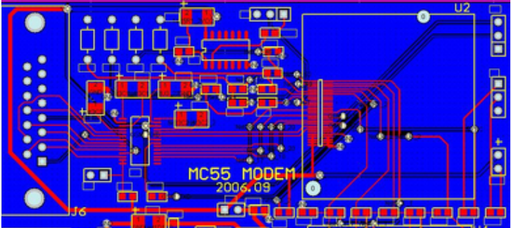
After scanning the surface image, set them as the top and bottom layers respectively, and convert them into bottom images that can be recognized by various copying software. According to the bottom images, first package the components (including small screen printing, pad aperture, and positioning holes, etc.) ), after all the components are finished, put them in the corresponding position, adjust the characters to make the font, font size and position consistent with the original board, and then proceed to the next step.
Use sandpaper to polish away the silk screen, ink and characters on the PCB surface to expose bright copper (there is an important trick to polish the pads-the polishing direction must be perpendicular to the scanning direction of the scanner). Of course, there is another method to heat the ink with alkaline liquid, but it takes a longer time. Usually the former method is more environmentally friendly and harmless to the human body. Having a clear and complete PCB bottom map is an important prerequisite for copying a good PCB board.
For a multi-layer PCB, the copy sequence is from outside to inside. Take an 8-layer board as an example:
First remove the first and eight layers of ink and copy the first and eight layers, then grind off the first and eight layers of copper, then copy the second and seventh layers, then the third and sixth layers, and finally copy the fourth and fifth layers. . During the operation, pay attention to the error between the scanned image and the real board, and it should be handled appropriately to make its size and direction consistent with the real board. After ensuring that the size of the base map is correct, start to adjust the position of the PCB components one by one to make them completely coincide with the base map, so that the next step is to place the vias, trace the wires and lay the copper. In this process, attention should be paid to details such as the width of the board, the size of the aperture, and the parameters of exposed copper.
Step 5: Check
A perfect inspection method will directly affect the quality of a PCB drawing. The use of image processing software, combined with PCB drawing software and the physical connection of the circuit can make a 100% accurate judgment. Impedance has a considerable influence on the high-frequency board. In the case of only the physical PCB, you can use an impedance tester to test or slice the PCB, measure the copper thickness and layer spacing with a metallurgical microscope, and analyze the dielectric of the substrate Constant (usually FR4, PTFE, RCC as the medium), so as to fully ensure that the PCB indicators are consistent with the original board.