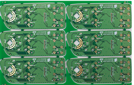
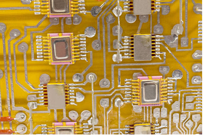
Since the insulating layer between the multilayer substrates is very thin, the impedance of 10 or 12 levels is very low on the circuit board layer and the first layer. As long as there is no problem in stacking or stacking, good signal integrity can be expected sex. It is more difficult to make the thickness of a 12-layer board of 62 mils, and there are not many things that can be processed by a 12-layer board PCB manufacturer.
Since the insulating layer always exists between the signal layer and the ring layer, it is not optimal to allocate the middle six layers to the signal lines in a ten-layer board design. Moreover, the signal layer adjacent to the loop layer is very important, that is, the PCB layout of signal, ground, signal, signal, power, ground, signal, signal, ground, and signal.
This design provides a suitable path for the signal current and its loop current. The appropriate wiring method is the first layer along the x-direction, the third layer along the Y-direction line, and the fourth layer along the x-direction. Visually, the 1st and 3rd layers are a pair of layered combinations, the 4th and 7th layers are a pair of layered combinations, and the 8th and 10th layers are the last layer of the layered combination. This is a pair.

If you need to change the direction of the line, you need to change the first layer of signal lines to the third layer after the "via". In fact, this may not always be the case, but please follow the design philosophy as much as possible.
Similarly, if the direction of the signal changes, it must be a through hole on the 8th and 10th layers or 4 to 7 layers. This arrangement makes the coupling between the forward path and the signal loop the tightest. For example, if the presence signal is a floor loop is in the second layer, if it is only in the second layer, then the signal on the first layer is transmitted in the third layer in the "through hole", so the loop is kept low inductance and low The capacity and high-quality characteristics of low electromagnetic shielding performance are retained in the second layer.
So if the actual route is not? For example, on layer 1, when the loop signal must look for the ground plane from the ninth layer, the loop current and the nearest ground via (the other component of the resistor and capacitor ground signal line pins, you will pass through up to 10 layers Hole. If you happen to have such a hole nearby, you are really lucky. If there is nothing near the available hole, the inductance will increase, the capacitance will decrease, and EMI will definitely increase.
The signal line, because if you need to pass through the hole to the wiring layer of the current pair, leaving another interconnection layer can be a cyclic signal back to the corresponding ground layer, you need to approach the hole near the underground hole. In layers 4 and 7, the signal loop returns from the power or ground plane because the capacitive coupling between the power and the ground plane is good and the signal is easy to transmit.
Design of multiple power layers
If the two power layers of the same voltage source require large output current, the circuit board must be woven into two sets of power and ground layers. In this case, an insulating layer is provided between each pair of power and ground layers. This provides us with the same two pairs of impedance power buses as ours. If the power layer stacking causes the impedance to be unequal, the shunt is not uniform, the transient voltage is much larger and the EMI increases sharply.
Remember that each pair of power and ground planes will be created for a different power source, because if the board has multiple different power supply voltages, multiple power planes are required. In either case, when determining the location of the printed circuit board power and ground planes, the manufacturer’s requirements for balanced structures must be kept in mind.