How to check the accuracy of PCB copy board
First: we first prepare at least three circuit boards of this electronic product;
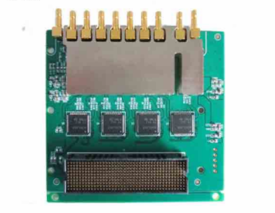
Second: Disassemble one of them and make a copy; the copy is carried out in three small steps (1): Know whether the MCU of this product needs program analysis, if you need to decrypt the cloned MCU program, you need to remove the MCU to save; (2 ) Copy the electronic components on the circuit board; measure; mark the position according to the components of the circuit board; (3) copy the PCB circuit diagram; perform circuit board proofing after copying (particularly note that the copied circuit board cannot be mass-produced immediately)

Third: Carry out the PCB production of the circuit diagram; make the circuit board; disassemble the circuit board components we have prepared; transplant to the new produced circuit board; then carry out the installation test! If the test is not done well; (1) first check whether the components are transplanted correctly; if the transplantation is correct, check whether the copied circuit diagram is wrong; if the transplanted installation test passes, it proves that the circuit board is copied correctly; (2) next we Purchase according to the copied electronic components; solder the purchased new components to the finished circuit board; then install the machine to test; if an abnormality is found; it proves that the components we purchased are not correct, we need to check two parts; the first check Whether the purchased component is consistent with the component we copied; secondly, check whether the copied component has a copy error position; after correcting the electronic component installation OK. (3) Next process the microcontroller program; crack the microcontroller program installation test; (Note: Cracking the single chip microcomputer is a tedious process); replace the completed new single chip with the already prepared circuit board for testing!
Fourth: After the errors of the sample are checked, the prototype will be made; we need to correct the errors in the process; avoid problems in the next production! After the data is corrected, we will make the prototype again; we will make the prototype again after the data is corrected. It can be mass-produced! Thanks for reading!
Second, the setting method of pcb teardrop
We often see the concept of teardrops, but many people say that they don’t understand the meaning of this word, let alone how to add teardrops to PCB design. Please look down with this question.
The role of teardrops
. Avoid breaking the contact point between the wire and the pad or the wire and the via hole when the circuit board is impacted by a huge external force, which can also make the PCB circuit board look more beautiful.
. When soldering, it can protect the pads, avoid the pads falling off during multiple soldering, and avoid uneven etching and cracks caused by the offset of the vias during production.
. Smooth the impedance during signal transmission, reduce the sharp jump of impedance, avoid reflections caused by the sudden decrease of line width during high-frequency signal transmission, and make the connection between the trace and the component pad tend to be smooth and transitional.
How to add teardrops
Execute the menu command "Tools-Teardrops" or the shortcut key "TE" to enter the teardrop attribute setting dialog box, and select the operation object:
. Working Mode-Add select to execute the add pcb teardrop command;
. Objects-All select matching objects, generally select "All" all; on the right as shown in the figure, the corresponding objects will be adapted, including "Via/TH PAD (via and through-hole pad)", "SMD Pad ( Patch pad)", "Track (wire)" and "T-Junction (T-type node)";
. Teardrop Style-Curved Teardrop shape selection curved complementary shape;
. Force Teardrops adopts a mandatory execution method for the operation of adding teardrops. Even if there is a DRC error, generally speaking, in order to ensure the complete addition of teardrops, we will check this item, and we can modify the DRC later;
. Adjust Teardrop Size When there is not enough space to add teardrops on the PCB circuit board, you can change the size of the teardrop to complete the action of adding teardrops more intelligently.