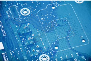
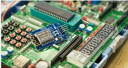
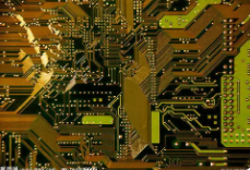
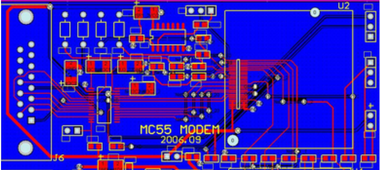
PCB circuit board is one of the most important components in the electronics industry today, and many electronic devices cannot do without it. PCB circuit board design not only directly affects the quality of the entire electronic product, but also has a great relationship with the cost, and can even affect the product's market share. It's not difficult to say, and it's not easy to say it. Pay attention to grasp the main points, and you can easily complete the PCB circuit board design.
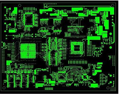
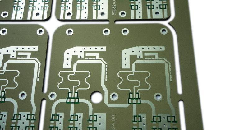
One, pay attention to the size and spacing of the pad
The minimum size of bonding pads (single wire) is 0.2mmX0.09mm90 degrees, and the minimum spacing of each pad is 2MILS. The width of the inner row of ground and power lines is also required to be 0.2mm. At the same time, the angle of the bonding pad should be adjusted according to the angle of the component pulling wire.
2. Pay attention to the distance between the pad and the original
The distance between SMT pads and DIE bonding pads and SMT components should be kept at least 0.3mm, and the distance between one DIE bonding pad and the other DIE should also be kept at least 0.2mm. The minimum signal trace is 2MILS, the spacing is 2MILS, and the main power trace is preferably 6-8MILS to enhance the strength of the substrate.

Three, pay attention to the relationship between vias, pads, traces and gold fingers
During routing, the vias should not be too close to the pads, traces, and gold fingers. The vias of the same attribute should be kept at least 0.12mm away from the gold fingers, and the vias of different attributes should be kept away from the pads and gold fingers. The minimum via hole should be 0.35mm for outer hole and 0.2mm for inner hole.
Four, pay attention to the production process of the substrate
Each wire must be electroplated to form copper pads and traces by electroplating. Even if there is no network pad, the pad must be copper-plated in a certain mode, otherwise it will appear. The result of no copper on the pad.
In summary, there are several points to note about PCB circuit board design. Mastering these points can make your PCB circuit board design smoother.
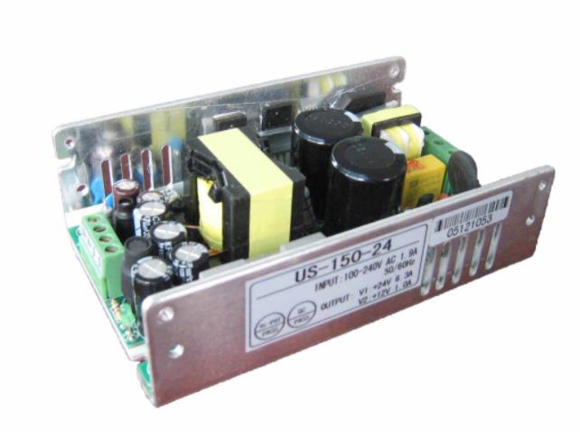
IPCB is a high-tech manufacturing enterprise focusing on the development and production of high-precision PCBs. iPCB is happy to be your business partner. Our business goal is to become the most professional prototyping PCB manufacturer in the world. Mainly focus on microwave high frequency PCB, high frequency mixed pressure, ultra-high multi-layer IC testing, from 1+ to 6+ HDI, Anylayer HDI, IC Substrate, IC test board, rigid flexible PCB, ordinary multi-layer FR4 PCB, etc. Products are widely used in industry 4.0, communications, industrial control, digital, power, computers, automobiles, medical, aerospace, instrumentation, Internet of Things and other fields.