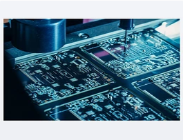
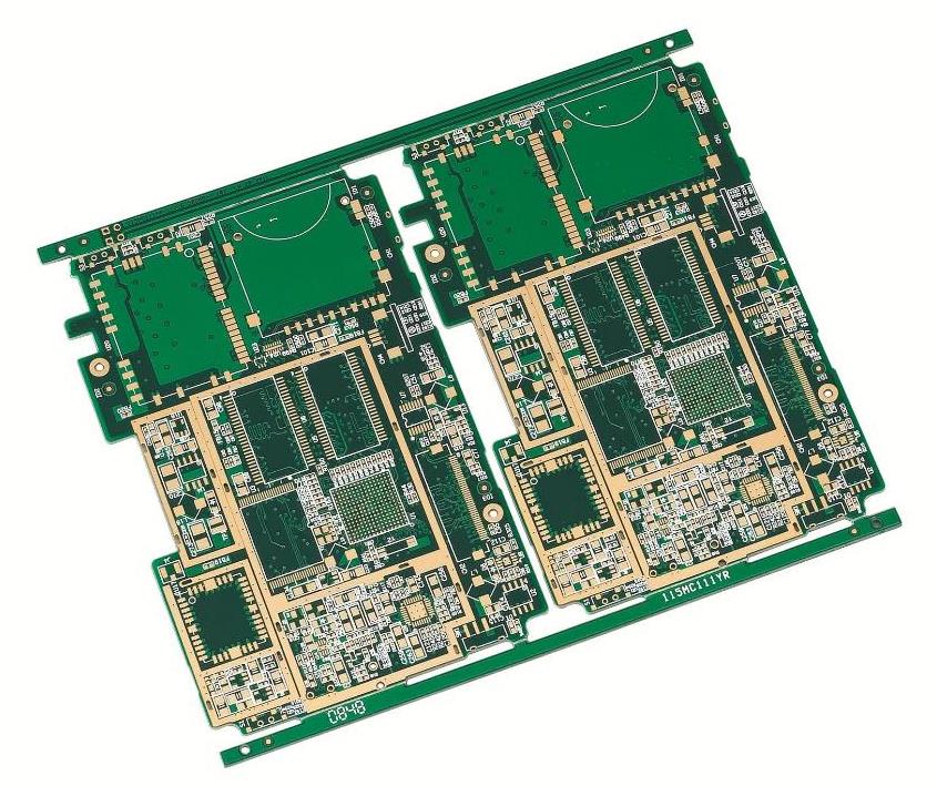
The basic principles of clock circuit PCB wiring, and the general requirements for clock circuit wiring are as follows.
1. Since the clock line is one of the factors that have the greatest impact on EMC, there should be fewer vias on the clock line; try to avoid running parallel with other signal lines, and keep it away from general signal lines to avoid interference with signal lines.
2. Avoid the power supply on the PCB board to prevent the power supply and the clock from interfering with each other.
3. When multiple clocks with different frequencies are used on a circuit board, two clock lines with different frequencies cannot run side by side. The circuit structure of the distribution network [9] is shown in Figure 8-6. This circuit uses a single clock source and distributes the clock signal to N remote destinations through a drive buffer.
A spider-shaped clock distribution network can always be distributed. A spider-shaped clock distribution network should pay attention to the following points.

1. The total load of the drive buffer circuit is R/N. For example, when using a 50Ω transmission line, a two-leg spider network, the total load on the driver end is 25Ω. There are not many drive buffer devices that can drive such a low load.
2. In order to drive more "spider legs", a more powerful clock driver is needed. A simple method is to connect the outputs of two or more drivers in parallel to form a high-power driver.
3. The total drive power required by the clock signal of the TTL circuit is 25 times that of the ECL circuit.
Clock distribution network with branch structure A circuit structure of clock distribution network with branch structure [9]. The circuit uses a single clock source, and distributes the clock signal to N inputs in a branch form through a drive buffer and a low-impedance clock distribution line. As the clock signal passes through each input, its rise time is stretched, and a small reflected pulse is also generated to propagate back to the source along the line. The reflected pulse is the derivative of the input signal and it will interfere with the reception. In order to reduce the amplitude of the reflected pulse, the following methods can be used.
1. Slow down the ascent speed of the drive, which can reduce the amplitude of the reflected pulse. The speed of the adopted driver can meet the requirement of clock skew.
2. Reduce the capacitance of each branch. In a multi-branch bus, the branch capacitance is related to the input capacitance of the clock receiver, the parasitic capacitance of the connector, and the capacitance of the PCB trace connecting the clock receiver.
3. Reduce the characteristic impedance (Zo) of the clock distribution line. The characteristic impedance of the clock distribution line is related to its geometric structure. The 50Ω clock line is 2.5 times more sensitive than the clock branch line capacitance of the 20Ω clock line. Reducing the distribution impedance helps prevent the clock drift from being affected by load changes.
The source termination structure using multiple clock lines is a circuit that uses a single clock driver to drive two source terminations [9. The impedance of the source termination circuit is twice that of the end termination circuit, and the required drive current drops to zero after 2T (T is the propagation delay), which reduces the average power consumption. One uses a single clock driver to drive two sources and uses multiple clock lines. The source end termination structure requires that the lines must be equal in length to ensure that the reflected pulses arrive at the same time; the load at each end must be equal to ensure that the reflected pulses have the same waveform. The source end termination resistance is related to the output impedance of the driver. The source end termination resistance is RS is the source termination resistance (Ω); Zo is the line impedance to be driven (Ω); Rdrive is the effective output impedance of the driver (Ω) ; N is the number of driven lines. It should be noted that in actual engineering, complete symmetry is difficult to achieve. If there is asymmetry in the line, the reflection and crosstalk of each line cannot be completely offset, which will cause the system to ring. Special crosstalk protection for the clock line.