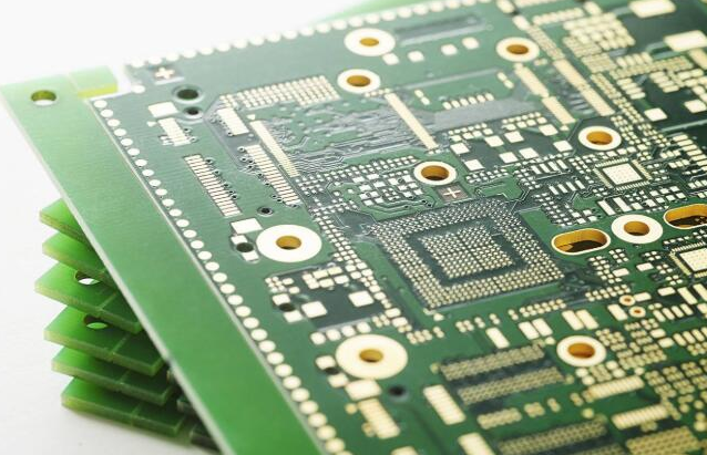
In the PCB production process, whether it is a single-layer, double-layer panel or a multi-layer board, one of the most basic and critical processes is graphics transfer, which transfers artwork graphics to copper foil substrates. Graphic transfer is a key control point in production, and it is also a technical problem. There are many PCB processing methods, such as screen printing pattern transfer process, dry film pattern transfer process, liquid photoresist pattern transfer process, electrodeposition photoresist (ED film) production process and laser direct imaging technology Can replace the dry film graphics transfer process. The liquid photoresist pattern transfer process is the first to be promoted. This process has the advantages of thin film, high resolution, low cost, and low requirements for operating conditions, and is widely used.
Application process flow chart of liquid photosensitive ink:

Surface treatment of substrate-coating (screen printing)-pre-baking-exposure-development-drying-inspection-etching-faded film-inspection (Note: inner panel)
Surface treatment of the substrate-coating (screen)-pre-baking-exposure-development-drying-inspection-plating-fading-etching-inspection (Note: outer panel)
Liquid photoresistor (liquid photoresist)
The liquid photo-liquid corrosion inhibitor (wet film) is made of photosensitive resin, photosensitizer, colorant, filler and solvent, etc., and obtains graphics after exposure. This is a negative sexy photo polymerization type. Compared with traditional corrosion-resistant inks and dry films, they have the following characteristics:
Compared with the dry film, the liquid wet film is correctly marked on the substrate, and can be filled with slight pits, scratches and other defects on the surface of the copper foil. Then the wet film is thinned to 5 to 10um, which is only about 1/3 of the dry film, and the upper layer of the wet film is not covered by the film (the upper layer of the dry film is covered with about 25um thick polyester cover film), so its graphics Sepsis, high clarity. For example, under the exposure time of 4S/7K, the destruction rate of dry film is 75um, while that of wet film is 40um. This can ensure the quality of the product.
PCB manufacturing is a liquid wet film with flexibility, which is particularly suitable for the production of flexible printed boards. For the increasingly popular electroless nickel plating process, the general dry film is not resistant to the gold plating solution, and the wet film is not resistant to the gold plating solution.
Wet film due to its own thickness reduction and material cost reduction, and compared with dry film, does not require a carrier polyester cover sheet (Polyester Cover sheet) and protective polyethylene membrane (Polyettylene Chemical Sheet), and there is no such thing as dry Membrane cutting and the like are treated as large waste, is there no need to deal with subsequent waste films?
In the past, when dry film was used, there were often up and down, electroplating, irregular lines, etc. The wet film is a liquid film that cannot be warped, leaked, and has neat lines. The allowable shelf time from the coating process to the display process is up to 48hr, which solves the contradiction between the PCB production process and improves the production efficiency. The wet film is a single liquid ink, which is easy to store and store. Generally, it is placed at a temperature of 20 to 2 degrees Celsius and a relative humidity of 55 to 5%. It is sealed and kept cooler. The storage period (storage LIFe): 4 to 6 months.
It has a wide range of uses. It can be used for the production of MLB inner line patterns and the production of electroplating patterns for perforated plates, and can also be used as a corrosion inhibitor for masking patterns in combination with the hole plugging process, and can also be used for the production of pattern templates. However, the uniformity of the wet film thickness (thickness) is not as good as that of the dry film. Is it difficult to grasp the degree of dryness after coating? In addition, the evaporation of additives, solvents, triggers, etc. in the wet film can pollute the environment, especially to PCB operators. Therefore, the PCB workplace must be well ventilated.