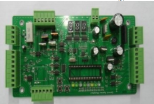
Before starting the PCB layout design, a complete and detailed description of the circuit is required, mainly in the following areas:
1: Schematic diagram, including component details, connection and edge connector specifications.
2: PCB component list, including component name, specification, model and manufacturer.
3: Mechanical specifications, including the size and shape of the circuit board, mounting holes, labels in areas where the component height is limited, and the location of edge connectors.
4: PCB printed circuit board specifications, single-sided, double-sided or multi-substrate, with or without holes.
5: Design specifications, including the type and size of pads, the width and spacing of wires.
6: Electrical specifications, such as the placement of components restricted by heat, the contribution of capacitance or inductance, grounding, critical wiring length, etc.

7: Data manipulation.
First, prepare a library, which describes the packaging type of each component required, including the form factor, pad type, size, and pad location. In the complete component form, the packaging type of each component used, the name and location of the component, and the connection surface on the printed circuit board should be indicated. The connection form gives an accurate description of all point-to-point connections. The final detailed information list of the board contains the board information and the x/y coordinates of the board corners. The correctness of the data in these tables, especially the importance of connecting tables, is very important. In many CAD systems, two independent operators are designated to connect the form to the same circuit. Only after eliminating the difference between the two connection forms, can proceed to the next step.
The schematic diagram provides a graphical representation of the functional processes and circuits. The first step in using a CAD system for PCB design is to enter the schematic. The schematic system includes:
1: Electrical connection (network);
2: Connection point;
3: Integrated circuit symbol;
4: Discrete PCB component symbols, such as resistors, capacitors, transistors, etc.
5: Input/output connector;
6: Power supply and grounding symbol;
7: Bus;
8: Non-connection symbol;
9: Component reference name;
10: Text description.
These symbols in the electrical schematic diagram should comply with international standards.
When obtaining the electrical schematic diagram, each graph opened is a separate "project management window". If you need to process multiple graphics at the same time, you can open them all, each of which has its own "project management window". The "Project Management" window is used to collect and organize all the resources needed for the project, including schematic folders, schematic events, parts libraries, parts, and output reports, such as lists and netlists. The management of the project does not actually include all resources, but only points to the various files needed by the project. Therefore, never delete or move files related to any items that are not found.